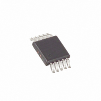
MAX5006BCUB+ Maxim Integrated Products, MAX5006BCUB+ Datasheet - Page 9

MAX5006BCUB+
Manufacturer Part Number
MAX5006BCUB+
Description
IC REG USB LDO 150MA 10-UMAX
Manufacturer
Maxim Integrated Products
Datasheet
1.MAX5005ACUBT.pdf
(13 pages)
Specifications of MAX5006BCUB+
Applications
Converter, USB
Voltage - Input
4 ~ 5.5 V
Number Of Outputs
1
Voltage - Output
3.3V
Operating Temperature
0°C ~ 70°C
Mounting Type
Surface Mount
Package / Case
10-MSOP, Micro10™, 10-uMAX, 10-uSOP
Polarity
Positive
Input Voltage Max
5.5 V
Output Voltage
3.3 V
Output Type
Fixed
Dropout Voltage (max)
0.4 V at 150 mA
Output Current
150 mA
Voltage Regulation Accuracy
3 %
Maximum Power Dissipation
0.444 W
Maximum Operating Temperature
+ 70 C
Mounting Style
SMD/SMT
Minimum Operating Temperature
0 C
Lead Free Status / RoHS Status
Lead free / RoHS Compliant
Note that some ceramic dielectrics exhibit large capac-
itance and ESR variation with temperature. With
dielectrics such as Z5U and Y5V, it may be necessary
to use 2.2µF or more to ensure stability at temperatures
below -10°C. With X7R or X5R dielectrics, 1µF should
be sufficient at all operating temperatures. Also, for
high-ESR tantalum capacitors, 2.2µF or more may be
needed to maintain stability. A graph of the Region of
Stable C
Typical Operating Characteristics.
To improve power-supply rejection and transient
response use a 1µF capacitor between IN and GND.
These devices are relatively immune to short-duration,
negative-going V
Characteristics section shows a graph of the Maximum
Pulse Duration vs. Reset Threshold Overdrive for which
reset is not asserted. The graph was produced using
negative going output transients starting at V
ending below the reset threshold by the magnitude
indicated (Reset Threshold Overdrive). The graph
shows the maximum pulse width that a negative going
V
reset pulse. As the amplitude of the transient increases
(i.e., goes further below the reset threshold), the maxi-
mum allowable pulse width decreases. Typically, a
V
threshold and lasts for 75µs will not trigger a reset
pulse.
The universal serial bus (USB) simplifies interconnectiv-
ity between peripheral devices and personal comput-
ers. USBs offer high-speed data communication rates
(up to 12Mbps) using only two lines (D+ and D-).
CMOS based USB peripherals that utilize deep submi-
cron technologies are more susceptible to electrostatic
discharge (ESD) failure due to shorter channel lengths,
shallower drain/source junctions, and lightly doped
drain structures. The MAX5005/MAX5006/MAX5007
incorporate a proprietary transient voltage suppression
(TVS) circuit for use with submicron devices.
The TVS design complies with IEC-1000-4-2 level 4
(EN61000-4-2) ±15kV Air Discharge and ±8kV Contact
Discharge as well as MIL STD 883C-Method 3015-6
level 3.
The TVS circuit handles up to 11A of surge current. The
TVS/ESD structure is directly coupled to the output of
the LDO regulator.
OUT
OUT
transient can typically have without triggering a
transient that goes only 10mV below the reset
150mA USB LDO Regulators with ±15kV TVS
USB ±15kV Transient Voltage
OUT
Negative-Going V
ESR vs. Load Current is shown in the
OUT
_______________________________________________________________________________________
transients. The Typical Operating
OUT
Suppression
Transients
OUT
and
Figure 2 shows the test circuit used to generate the
8/40µs short circuit waveform of Figure 3. Figures 4, 5,
and 6 show the actual surge current I/V characteristics
with various capacitive loads.
The MAX5005/MAX5006/MAX5007 are characterized
to the following limits on D+, D-, and IN:
• ±15kV using the Human Body Model
• ±8kV using the Contact Discharge Method specified
• ±15kV using the Air-Gap Discharge Method speci-
Note that in order to achieve the above ESD levels on
IN, a ceramic 1µF ceramic capacitor should be con-
nected from IN to GND.
ESD performance depends on several conditions.
Contact Maxim for a reliability report that documents
test setup, methodology, and results.
Figure 7 shows the Human Body Model, and Figure 8
shows the current waveform it generates when dis-
charged into low impedance. This model consists of a
100pF capacitor charged to the ESD voltage of interest,
which is then discharged into the test device through a
1.5k resistor.
Figure 9 shows the test circuit used for transmission
line pulsing conditions. The 200ns pulsewidth has a
rise time of 4ns. Figure 10 shows the Current vs.
Voltage characteristics for various output capacitance
values.
in IEC 1000-4-2 (EN61000-4-2)
fied in IEC 1000-4-2 (EN61000-4-2).
ESD Transmission Line Pulsing
TVS Surge Test Information
and µP Reset
ESD Test Conditions
Human Body Model
ESD Performance
9


