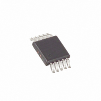
MAX5006BCUB+ Maxim Integrated Products, MAX5006BCUB+ Datasheet - Page 8

MAX5006BCUB+
Manufacturer Part Number
MAX5006BCUB+
Description
IC REG USB LDO 150MA 10-UMAX
Manufacturer
Maxim Integrated Products
Datasheet
1.MAX5005ACUBT.pdf
(13 pages)
Specifications of MAX5006BCUB+
Applications
Converter, USB
Voltage - Input
4 ~ 5.5 V
Number Of Outputs
1
Voltage - Output
3.3V
Operating Temperature
0°C ~ 70°C
Mounting Type
Surface Mount
Package / Case
10-MSOP, Micro10™, 10-uMAX, 10-uSOP
Polarity
Positive
Input Voltage Max
5.5 V
Output Voltage
3.3 V
Output Type
Fixed
Dropout Voltage (max)
0.4 V at 150 mA
Output Current
150 mA
Voltage Regulation Accuracy
3 %
Maximum Power Dissipation
0.444 W
Maximum Operating Temperature
+ 70 C
Mounting Style
SMD/SMT
Minimum Operating Temperature
0 C
Lead Free Status / RoHS Status
Lead free / RoHS Compliant
150mA USB LDO Regulators with ±15kV TVS
and µP Reset
brownout conditions. Reset is guaranteed to be logic
high or low depending on the device chosen (see
Ordering Information). RESET or RESET asserts when
V
ed for at least 100ms minimum after V
the reset threshold. RESET or RESET also asserts when
MR is pulled low.
When reset is not asserted a logic high to SELR con-
nects a 1.5k
full speed USB peripherals and a logic low connects a
1.5k
peripherals. Logic low on ENR enables the selected
termination resistor connection and logic high disables
the selected termination resistor connection. An assert-
ed reset always disconnects the termination resistors.
D+ and D- include transient voltage suppressors rated
at ±15kV (see USB ±15kV Transient Voltage
Suppression section).
The proprietary TVS shunt circuit passes no data
through the MAX5005/MAX5006/MAX5007, thereby
eliminating delays associated with series protection cir-
cuits. D+ and D- have only 1µA of leakage current and
a typical input capacitance of 40pF at 1MHz.
Many µP-based products require manual reset capabil-
ity, allowing the operator, a test technician, or external
logic circuitry to initiate a reset. A logic low on MR
asserts a reset while the regulator output voltage is still
within tolerance.
Reset remains asserted while MR is low and for the
reset timeout period (100ms minimum) after MR returns
high. The MR input has an internal pullup of 25k
to OUT. Drive this input with TTL/CMOS logic levels or
with open-drain/collector outputs. Connect a normally
open momentary switch from MR to GND to create a
manual reset function; external debounce circuitry is
not required. If MR is driven from long cables or the
device is used in a noisy environment, connect a 0.1µF
capacitor from MR to GND to provide additional noise
immunity. For proper operation, ensure that the voltage
on MR is not greater than a diode drop above V
An internal circuit monitors the input and output volt-
ages. When the output voltage is greater than the input
voltage, the internal pass transistor and parasitic
diodes turn off, and OUT powers the device. There is
no leakage path from OUT to IN. Therefore, the output
8
OUT
_______________________________________________________________________________________
is below the reset threshold and remains assert-
termination resistor from D- to OUT for low-speed
Output to Input Reverse Leakage
termination resistor from D+ to OUT for
Manual Reset Input
SELR and ENR
OUT
Protection
D+ and D-
rises above
OUT
(typ)
.
can be powered from an auxiliary supply such as a
backup battery without any need for additional blocking
diodes.
The MAX5005/MAX5006/MAX5007 include a current
limiter that monitors and controls the pass transistor’s
gate voltage, limiting the output current to 350mA (typ).
For design purposes, consider the current limit to be
160mA (min) to 600mA (max). The output can be short-
ed to ground for an indefinite period without damaging
the part.
When the junction temperature exceeds T
an internal thermal sensor signals the shutdown logic,
turning off the pass transistor and allowing the IC to
cool. The thermal sensor turns the pass transistor on
again after the IC’s junction temperature decreases by
20°C, resulting in a pulsed output during continuous
thermal overload conditions. Thermal overload protec-
tion is designed to protect the MAX5005/MAX5006/
MAX5007 in the event of fault conditions. For continu-
ous operation, do not exceed the absolute maximum
junction temperature rating of T
The MAX5005/MAX5006/MAX5007’s maximum power
dissipation depends on the thermal resistance of the
case and circuit board, the temperature difference
between the die junction and the ambient air, and the
rate of airflow. The power dissipation across the device
is P = I
tion is:
where T
the die junction and the surrounding air,
mal resistance of the package from junction to ambient.
The MAX5005/MAX5006/MAX5007’s ground pin (GND)
performs the dual function of providing an electrical
connection to the system ground and channeling heat
away. Connect GND to the system ground using a
large pad or ground plane. For optimum performance,
minimize trace inductance to D+, D-, and GND.
For stable operation over the full temperature range
and with load currents up to 150mA, use a 1µF (min)
output capacitor. To reduce noise and improve load
transient response, stability, and power-supply rejec-
tion, use large output capacitor values such as 10µF.
Operating Region and Power Dissipation
OUT
J
- T
Capacitor Selection and Regulator
(V
A
IN
is the temperature difference between
P
Applications Information
- V
MAX
OUT
= (T
). The maximum power dissipa-
J
- T
A
Thermal Protection
J
) / (
= +150°C.
JA
Current Limit
)
JA
J
Stability
= +160°C,
is the ther-


