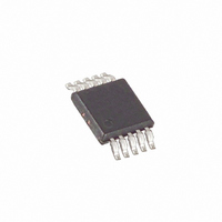
MAX5006BCUB+ Maxim Integrated Products, MAX5006BCUB+ Datasheet - Page 2

MAX5006BCUB+
Manufacturer Part Number
MAX5006BCUB+
Description
IC REG USB LDO 150MA 10-UMAX
Manufacturer
Maxim Integrated Products
Datasheet
1.MAX5005ACUBT.pdf
(13 pages)
Specifications of MAX5006BCUB+
Applications
Converter, USB
Voltage - Input
4 ~ 5.5 V
Number Of Outputs
1
Voltage - Output
3.3V
Operating Temperature
0°C ~ 70°C
Mounting Type
Surface Mount
Package / Case
10-MSOP, Micro10™, 10-uMAX, 10-uSOP
Polarity
Positive
Input Voltage Max
5.5 V
Output Voltage
3.3 V
Output Type
Fixed
Dropout Voltage (max)
0.4 V at 150 mA
Output Current
150 mA
Voltage Regulation Accuracy
3 %
Maximum Power Dissipation
0.444 W
Maximum Operating Temperature
+ 70 C
Mounting Style
SMD/SMT
Minimum Operating Temperature
0 C
Lead Free Status / RoHS Status
Lead free / RoHS Compliant
ABSOLUTE MAXIMUM RATINGS
IN to GND .................................................................-0.3V to +6V
D+, D- to GND..........................................................-0.3V to +6V
MR to GND ..............................................-0.3V to (V
RESET, RESET to GND, Push-Pull............-0.3V to (V
RESET to GND, Open-Drain.....................................-0.3V to +6V
OUT, SELR, ENR to GND .........................................-0.3V to +6V
Maximum Current to Any Pin
ELECTRICAL CHARACTERISTICS
(V
150mA USB LDO Regulators with ±15kV TVS
and µP Reset
Stresses beyond those listed under “Absolute Maximum Ratings” may cause permanent damage to the device. These are stress ratings only, and functional
operation of the device at these or any other conditions beyond those indicated in the operational sections of the specifications is not implied. Exposure to
absolute maximum rating conditions for extended periods may affect device reliability.
2
Input Voltage Range
Supply Current
REGULATOR
Guaranteed Output Current
Output Voltage
Dropout Voltage (Note 2)
Output Current Limit
Input Reverse Leakage Current
Startup Response Time
Thermal Shutdown Temperature
Thermal Shutdown Hysteresis
RESET CIRCUIT
Reset Threshold (Note 3)
Reset Timeout Period
V
MR Input Voltage
MR Minimum Input Pulse Width
MR Glitch Rejection
MR to Reset Delay
MR Pullup Resistance to OUT
SELR Input Voltage
IN
(except IN, OUT, D+, D-).............................................± 20mA
OUT
_______________________________________________________________________________________
= +5V, I
to Reset Delay
PARAMETER
OUT
= 0, C
OUT
= 2.2µF, T
SYMBOL
A
T
V
T
I
JSHDN
= 0°C to +70°C, unless otherwise noted. Typical specifications are at T
I
GND
V
V
OUT
t
V
V
V
t
V
V
JSHD N
OUT
RD
RP
TH
IN
IH
IH
DO
IL
IL
I
Measured at GND
V
I
I
V
V
Rising edge of V
R
MAX500_ACUB
MAX500_BCUB
Connects R
Connects R
LOAD
LOAD
LOAD
IN
IN
IN
L
OUT
OUT
= 500
= 4.0V to 5.5V, I
= 5.5V
= 0, V
= 100mA
= 10mA
= 150mA
+ 0.3V)
+ 0.3V)
OUT
TERM
TERM
= 5.5V
CONDITIONS
IN
to D-
to D+
to V
OUT
Short-Circuit Duration ....................................................Indefinite
Continuous Power Dissipation (T
Thermal Resistance (
Operating Temperature Range...............................0°C to +70°C
Junction Temperature ......................................................+150°C
Storage Temperature Range .............................-65°C to +150°C
Lead Temperature (soldering, 10s) .................................+300°C
OUT
10-Pin µMAX (derate 5.6mW/°C above +70°C) ...........444mW
= 0 to 100mA
JA
)...............................................180°C/W
V
V
0.8 x
0.8 x
2.92
2.75
MIN
150
165
100
4.0
3.2
OUT
10
OUT
1
A
= +70°C)
TYP
3.05
2.89
300
350
500
160
200
120
500
3.3
25
20
20
75
25
1
A
= +25°C.) (Note 1)
V
V
MAX
0.2 x
0.2 x
3.18
3.01
400
300
5.5
3.4
50
30
OUT
45
OUT
UNITS
mA
mV
mA
ms
k
µA
µA
µs
o
o
µs
µs
ns
ns
V
V
V
V
V
C
C


