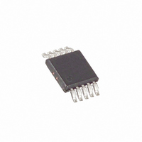
MAX5006BCUB+ Maxim Integrated Products, MAX5006BCUB+ Datasheet - Page 3

MAX5006BCUB+
Manufacturer Part Number
MAX5006BCUB+
Description
IC REG USB LDO 150MA 10-UMAX
Manufacturer
Maxim Integrated Products
Datasheet
1.MAX5005ACUBT.pdf
(13 pages)
Specifications of MAX5006BCUB+
Applications
Converter, USB
Voltage - Input
4 ~ 5.5 V
Number Of Outputs
1
Voltage - Output
3.3V
Operating Temperature
0°C ~ 70°C
Mounting Type
Surface Mount
Package / Case
10-MSOP, Micro10™, 10-uMAX, 10-uSOP
Polarity
Positive
Input Voltage Max
5.5 V
Output Voltage
3.3 V
Output Type
Fixed
Dropout Voltage (max)
0.4 V at 150 mA
Output Current
150 mA
Voltage Regulation Accuracy
3 %
Maximum Power Dissipation
0.444 W
Maximum Operating Temperature
+ 70 C
Mounting Style
SMD/SMT
Minimum Operating Temperature
0 C
Lead Free Status / RoHS Status
Lead free / RoHS Compliant
ELECTRICAL CHARACTERISTICS (continued)
(V
Note 1: All devices are 100% tested at T
Note 2: Dropout voltage is defined as V
Note 3: Specification is guaranteed to ±4 limit.
SELR Input Current
ENR Input Voltage
ENR Input Current
Open-Drain RESET Output Low
Voltage (MAX5005)
Open-Drain Reset Output Leakage
Current (MAX5005)
Push-Pull RESET Output Voltage
(MAX5006)
Push-Pull RESET Output Voltage
(MAX5007)
USB OPTIONS AND TRANSIENT SUPPRESSION
D+/D- R
D+/D- Input Leakage Current
D+ to D- Capacitance
D+, D- Capacitance to GND
ESD Trigger Voltage
Surge Trigger Voltage
Clamping Voltage
Surge Current
D+/D- to GND ESD
IN
= +5V, I
150mA USB LDO Regulators with ±15kV TVS
tested.
TERM
PARAMETER
OUT
Impedance
= 0, C
_______________________________________________________________________________________
OUT
= 2.2µF, T
SYMBOL
A
= 0°C to +70°C, unless otherwise noted. Typical specifications are at T
I
V
V
V
V
V
IN
V
LKG
V
A
OH
OH
OL
OL
OL
IH
IL
- V
= +25 C. Limits over temperature are guaranteed by characterization and not production
OUT
SELR = GND or OUT
R
R
ENR = GND or OUT
V
V
Reset not asserted
V
V
asserted
V
reset not asserted
V
reset not asserted
V
asserted
ENR = GND, SELR = GND or OUT
V
1MHz, 100mVp-p signal
applied at D+ and D-,
V
1MHz, 100mVp-p signal
applied at D+ and D-,
V
dV/dt < 1V/ns, V
dV/dt < 2V/ s, V
6A, pulse width = 200ns to 40 s
16V, pulse width = 200ns to 40 s
Human Body Model MIL-STD-883
Contact Discharge IEC1000-4-2
(EN61000-4-2)
Air Discharge IEC1000-4-2 (EN61000-4-2)
when V
OUT
OUT
OUT
OUT
OUT
OUT
OUT
ENR
OUT
OUT
TERM
TERM
= V
> 1.0V, I
> 2.7V, I
= 1.0V, I
> V
> V
> V
= 1.0V, I
= 3.3V
= 3.3V
enabled
disabled
OUT
OUT
TH(MIN)
TH(MAX)
TH(MAX)
is 2% below the value of V
= 3.3V
SINK
SINK
SINK
SOURCE
CONDITIONS
D+
D+
, I
, I
, I
SINK
SOURCE
SINK
= 50 A, reset asserted
= 3.2mA, reset asserted
= 50 A, reset asserted
or V
or V
= 150 A, reset
= 3.2mA, reset
D-
D-
= 3.2mA,
> 3.6V
> 3.6V
= 500 A,
ENR = OUT
Unpowered
ENR = OUT
Unpowered
OUT
for V
and µP Reset
IN
V
V
V
0.8 x
0.8 x
0.8 x
1425
MIN
-1.0
3.6
3.6
OUT
OUT
OUT
-1
-1
-1
= V
OUT
1500
TYP
+ 1V.
5.5
24
40
47
16
16
5
16
15
A
6
8
= +25°C.) (Note 1)
V
MAX
1575
0.2 x
0.3
0.4
1.0
0.3
0.4
0.4
OUT
1
1
1
UNITS
pF
pF
kV
V
V
V
V
V
V
V
A
A
A
A
A
3


