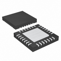
MAX8550ETI+T Maxim Integrated Products, MAX8550ETI+T Datasheet - Page 25

MAX8550ETI+T
Manufacturer Part Number
MAX8550ETI+T
Description
IC PWR SUP DDR INTEG 28TQFN
Manufacturer
Maxim Integrated Products
Datasheet
1.MAX8550ETIT.pdf
(29 pages)
Specifications of MAX8550ETI+T
Applications
Controller, DDR
Voltage - Input
2 ~ 28 V
Number Of Outputs
2
Voltage - Output
1.8V, 2.5V, 0.7 ~ 5.5 V
Operating Temperature
-40°C ~ 85°C
Mounting Type
Surface Mount
Package / Case
28-TQFN Exposed Pad
Output Voltage
0.7 V to 5.5 V, 1.8 V, 2.5 V
Output Current
20 A
Input Voltage
2 V to 28 V
Mounting Style
SMD/SMT
Maximum Operating Temperature
+ 85 C
Minimum Operating Temperature
- 40 C
Lead Free Status / RoHS Status
Lead free / RoHS Compliant
The output sag is also a function of the maximum duty
factor, which can be calculated from the on-time and
minimum off-time:
where t
Electrical Characteristics) and K is from Table 1.
The overshoot during a full-load to no-load transient
due to stored inductor energy can be calculated as:
The output-voltage adjustable range for continuous-
conduction operation is restricted by the nonadjustable
minimum off-time one-shot. For best dropout perfor-
mance, use the slower (200kHz) on-time setting. When
working with low input voltages, the duty-factor limit
must be calculated using worst-case values for on- and
off-times. Manufacturing tolerances and internal propa-
gation delays introduce an error to the TON K-factor.
This error is greater at higher frequencies (see Table
1). Also, keep in mind that transient-response perfor-
mance of buck regulators operated too close to
dropout is poor, and bulk output capacitance must
often be added (see the V
Procedure section).
The absolute point of dropout is when the inductor cur-
rent ramps down during the minimum off-time (∆I
as much as it ramps up during the on-time (∆I
ratio h = ∆I
to slew the inductor current higher in response to
increased load, and must always be greater than 1. As
h approaches 1, the absolute minimum dropout point,
the inductor current cannot increase as much during
each switching cycle, and V
unless additional output capacitance is used.
A reasonable minimum value for h is 1.5, but adjusting
this up or down allows trade-offs between V
capacitance, and minimum operating voltage. For a
given value of h, the minimum operating voltage can be
calculated as:
V
SAG
=
OFF(MIN)
2
C
L
UP
Integrated DDR Power-Supply Solutions for
OUT
V
×
SOAR
/ ∆I
∆
Applications Information
I
Desktops, Notebooks, and Graphic Cards
×
LOAD MAX
DOWN
______________________________________________________________________________________
Dropout Performance (Buck)
is the minimum off-time (see the
V
=
OUT
(
∆
2
I
⎡
⎢
⎢
⎣
×
LOAD MAX
indicates the controller’s ability
(
)
V
C
2
IN
SAG
OUT
⎡
⎢
⎣
V
-
(
OUT
V
SAG
OUT
V
equation in the Design
IN
V
×
IN
)
2
×
)
V
greatly increases,
OUT
×
×
K
K
L
+
+
t
OFF MIN
SAG
t
OFF MIN
UP
(
, output
DOWN
(
). The
)
⎤
⎥
⎦
)
⎤
⎥
⎥
⎦
)
where V
drops in the discharge and charge paths (see the On-
Time One-Shot (TON) section), t
Electrical Characteristics, and K is taken from Table 1.
The absolute minimum input voltage is calculated with
h = 1.
If the calculated V
minimum input voltage, then the operating frequency
must be reduced or output capacitance added to
obtain an acceptable V
anticipated, calculate V
transient response.
A dropout design example follows:
V
f
K = 1.7µs
t
V
h = 1.5
In applications where fast-load transients occur, the
output voltage changes instantly by R
∆I
put capacitors for such applications, and maximizes
the output-voltage AC and DC tolerance window in
tight-tolerance applications.
Figure 9 shows the connection of OUT and FB in a volt-
age-positioned circuit. In nonvoltage-positioned cir-
cuits, the MAX8550/MAX8551 regulate at the output
capacitor. In voltage-positioned circuits, the MAX8550/
MAX8551 regulate on the inductor side of the voltage-
positioning resistor. V
SW
OFF(MIN)
OUT
DROP1
V
LOAD
V
IN MIN
IN MIN
V
= 600kHz
(
(
OUT VPS
= 2.5V
. Voltage positioning allows the use of fewer out-
)
)
DROP1
= V
(
=
= 450ns
=
DROP2
⎡
⎢
⎢
⎢
⎢
⎢
⎣
⎡
⎢
⎢
⎢
⎢
⎢
⎣
)
1 -
1
-
=
V
and V
⎛
⎜
⎝
OUT
⎛
⎜
⎝
2 5
h
1 5
V
.
.
IN(MIN)
= 100mV
OUT NO LOAD
V
×
V
Voltage Positioning (Buck)
OUT
×
1 7
+
DROP2
×
t
.
(
SAG
OFF MIN
V
K
0 1
µ
450
DROP
SAG
.
s
is reduced to:
_
is greater than the required
(
V
. If operation near dropout is
ns
are the parasitic voltage
1
to be sure of adequate
)
⎞
⎟
⎠
⎤
⎥
⎥
⎥
⎥
⎥
⎦
⎞
⎟
⎠
)
⎤
⎥
⎥
⎥
⎥
⎥
⎦
+
OFF(MIN)
-
+
0 1
R
V
.
DROP
POS
V
ESR
-
0 1
2
×
.
is from the
V
-
× C
I
LOAD
V
=
DROP
OUT
4 3
.
V
25
1
×


