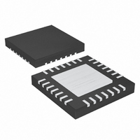
MAX8550ETI+T Maxim Integrated Products, MAX8550ETI+T Datasheet - Page 23

MAX8550ETI+T
Manufacturer Part Number
MAX8550ETI+T
Description
IC PWR SUP DDR INTEG 28TQFN
Manufacturer
Maxim Integrated Products
Datasheet
1.MAX8550ETIT.pdf
(29 pages)
Specifications of MAX8550ETI+T
Applications
Controller, DDR
Voltage - Input
2 ~ 28 V
Number Of Outputs
2
Voltage - Output
1.8V, 2.5V, 0.7 ~ 5.5 V
Operating Temperature
-40°C ~ 85°C
Mounting Type
Surface Mount
Package / Case
28-TQFN Exposed Pad
Output Voltage
0.7 V to 5.5 V, 1.8 V, 2.5 V
Output Current
20 A
Input Voltage
2 V to 28 V
Mounting Style
SMD/SMT
Maximum Operating Temperature
+ 85 C
Minimum Operating Temperature
- 40 C
Lead Free Status / RoHS Status
Lead free / RoHS Compliant
a divider current of approximately 10µA to prevent signifi-
cant inaccuracy in the valley current-limit tolerance.
Alternately, foldback current limit can be implemented
if the UVP latch option is not available. Foldback cur-
rent limit reduces the power dissipation of external
components so they can withstand indefinite overload
and short circuit, with automatic recovery after the over-
load or short circuit is removed. To implement foldback
current limit, connect a resistor from V
in Figure 7 and the Typical Applications Circuit), in
addition to the resistor-divider network (R4 and R5)
used for setting the adjustable current limit as shown in
Figure 7.
The following is a procedure for calculating the value of
R4, R5, and R6:
1) Calculate the voltage, V
2) Pick a percentage of foldback, PFB, from 15%
3) Calculate the voltage, V
Figure 7. Foldback Current Limit
when the output voltage is at nominal:
to 40%.
shorted (0V):
V
ILIM NOM
(
Integrated DDR Power-Supply Solutions for
MAX8550/
MAX8551
)
Desktops, Notebooks, and Graphic Cards
=
______________________________________________________________________________________
10
×
GND
ILIM
REF
R
×
DS ON Q
I
LOAD MAX
(
ILIM(0V)
ILIM(NOM)
)
Foldback Current Limit
C
(
REF
2
, when the output is
)
, required at ILIM
R6
R4
×
OUT
⎛
⎜
⎝
1
V
OUT
-
to ILIM (R6
LIR
R5
2
⎞
⎟
⎠
4) The value for R4 can be calculated as:
5) The parallel combination of R5 and R6, denoted
6) Then R6 can be calculated as:
7) Then R5 is calculated as:
A low-current Schottky diode, such as the CMDSH-3
from Central Semiconductor, works well for most appli-
cations. Do not use large-power diodes, because high-
er junction capacitance can charge up the voltage at
BST to the LX voltage and this exceeds the absolute
maximum rating of 6V. The boost capacitor should be
0.1µF to 4.7µF, depending on the input and output volt-
ages, external components, and PC board layout. The
boost capacitance should be as large as possible to
prevent it from charging to excessive voltage, but small
enough to adequately charge during the minimum low-
side MOSFET conduction time, which happens at maxi-
mum operating duty cycle (this occurs at minimum
input voltage). In addition, ensure that the boost capac-
itor does not discharge to below the minimum gate-to-
source voltage required to keep the high-side MOSFET
R56, is calculated as:
R
6
=
⎡
⎢
⎢
⎢
⎣
(
(
(
V
V
OUT
V
ILIM NOM
ILIM V
(
-
(
R
0
R
(
V
4
56
R
V
ILIM NOM
)
=
Capacitor Selection (Buck)
OUT
5
=
)
=
=
2
(
−
V
R
P
⎛
⎜
⎝
R
Boost-Supply Diode and
FB
6
10
×
V
6
2
-
ILIM V
10
V
×
µ
)
-
V
R
×
-
ILIM V
A
µ
4
R
R
V
(
A
⎞
⎟
⎠
0
56
ILIM V
V
56
×
ILIM NOM
(
-
)
0
)
R
R
(
0
5
)
×
(
4
6
)
R
)
)
56
)
×
)
R
4 -
⎤
⎥
⎥
⎥
⎦
23


