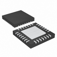
MAX8550ETI+T Maxim Integrated Products, MAX8550ETI+T Datasheet - Page 16

MAX8550ETI+T
Manufacturer Part Number
MAX8550ETI+T
Description
IC PWR SUP DDR INTEG 28TQFN
Manufacturer
Maxim Integrated Products
Datasheet
1.MAX8550ETIT.pdf
(29 pages)
Specifications of MAX8550ETI+T
Applications
Controller, DDR
Voltage - Input
2 ~ 28 V
Number Of Outputs
2
Voltage - Output
1.8V, 2.5V, 0.7 ~ 5.5 V
Operating Temperature
-40°C ~ 85°C
Mounting Type
Surface Mount
Package / Case
28-TQFN Exposed Pad
Output Voltage
0.7 V to 5.5 V, 1.8 V, 2.5 V
Output Current
20 A
Input Voltage
2 V to 28 V
Mounting Style
SMD/SMT
Maximum Operating Temperature
+ 85 C
Minimum Operating Temperature
- 40 C
Lead Free Status / RoHS Status
Lead free / RoHS Compliant
attained when SS reaches approximately 1.6V. This
lowering of the current limit during startup limits the ini-
tial inrush current peaks, particularly when driving
capacitors. Choose the value of the SS cap appropri-
ately to set the soft-start time window. Leave SS floating
to disable the soft-start feature.
POK1 is an open-drain output for a window comparator
that continuously monitors V
low when SHDNA is low and during the buck regulator
output’s soft-start. After the digital soft-start terminates,
POK1 becomes high impedance as long as the output
voltage is within ±10% of the nominal regulation voltage
set by FB. When V
above the nominal regulation voltage, the MAX8550/
MAX8551 pull POK1 low. Any fault condition forces
POK1 low until the fault latch is cleared by toggling
SHDNA or cycling AV
output voltages, connect an external pullup resistor
between POK1 and AV
in most applications. Note that the POK1 window detec-
tor is completely independent of the overvoltage and
undervoltage-protection fault detectors and the state of
VTTS and VTTR.
The SHDNA input corresponds to the buck regulator
and places the buck regulator’s portion of the IC in a
low-power mode (see the Electrical Characteristics
table). SHDNA is also used to reset a fault signal such
as an overvoltage or undervoltage fault.
When output discharge is enabled, (OVP/UVP = AV
or open) and SHDNA and SHDNB are pulled low, or if
UVP is enabled (OVP/UVP = AV
70% of its regulation set point, the MAX8550 dis-
charges the buck regulator output (through the OUT
input) through an internal 10Ω switch to ground. While
the output is discharging, DL is forced low and the
PWM controller is disabled but the reference remains
Integrated DDR Power-Supply Solutions for
Desktops, Notebooks, and Graphic Cards
Table 2. Shutdown and Standby Control Logic
16
______________________________________________________________________________________
STBY
AV
GND
GND
GND
GND
DD
SHDNA and Output Discharge
OUT
DD
DD
drops 10% below or rises 10%
power below 1V. For logic-level
SHDNA
. A 100kΩ resistor works well
AV
AV
AV
GND
GND
OUT
DD
DD
DD
. POK1 is actively held
Power-OK (POK1)
DD
) and V
OUT
SHDNB
AV
AV
AV
GND
GND
DD
DD
DD
falls to
DD
active to provide an accurate threshold. Once the out-
put voltage drops below 0.3V, the MAX8550 shuts
down the reference and pulls DL high, effectively
clamping the buck output and LX to ground.
When output discharge is disabled (OVP/UVP = REF or
GND), the controller does not actively discharge the
buck output and the DL driver remains low. Under these
conditions, the buck output discharge rate is determined
by the load current and its output capacitance. The buck
regulator detects and latches the discharge-mode state
set by the OVP/UVP setting on startup.
For the MAX8551, the OVP/UVP is internally connected
to REF, which permanently enables the output dis-
charge feature (see Table 1).
The SHDNB input corresponds to the VTT and VTTR
outputs, and when driven low, places the linear-regula-
tor portion of the IC in a low-power mode (see the
Electrical Characteristics table). When SHDNB is pulled
low, VTT and VTTR are high impedance.
The STBY input is an active-high input that is used to
shut down only the VTT output. When STBY is high, VTT
is high impedance. The STBY input overrides the
SHDNB input, so even with SHDNB high, if STBY is
high, then the VTT output is inactive.
POK2 is the open-drain output for a window compara-
tor that continuously monitors the VTTS input and VTTR
output. POK2 is pulled low when REFIN is less than
0.8V, or when SHDNB is pulled low. POK2 is high
impedance as long as the output voltage is within
±10% of the nominal regulation voltage as set by
REFIN. When V
below its nominal regulation voltage, the MAX8550/
MAX8551 pull POK2 low. For logic-level output volt-
ages, connect an external pullup resistor between
POK2 and AV
applications.
BUCK OUTPUT
OFF
OFF
ON
ON
ON
DD
VTTS
. A 100kΩ resistor works well in most
or V
VTT
OFF
OFF
OFF
VTTR
ON
ON
rises 10% above or 10%
SHDNB and STBY
Power-OK (POK2)
VTTR
OFF
OFF
ON
ON
ON


