NCP4208MNR2G ON Semiconductor, NCP4208MNR2G Datasheet - Page 17
NCP4208MNR2G
Manufacturer Part Number
NCP4208MNR2G
Description
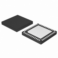
IC CTLR 8PH VR11.1 PMBUS 48-QFN
Manufacturer
ON Semiconductor
Datasheet
1.NCP4208MNR2G.pdf
(30 pages)
Specifications of NCP4208MNR2G
Applications
Controller, Intel VR11.1
Voltage - Input
4.7 ~ 5.75 V
Number Of Outputs
8
Voltage - Output
0.16 ~ 5 V
Operating Temperature
0°C ~ 85°C
Mounting Type
Surface Mount
Package / Case
48-TQFN Exposed Pad
Output Voltage
0.375 V to 1.6 V
Input Voltage
0.3 V to 6 V
Switching Frequency
1.5 MHz
Operating Temperature Range
0 C to + 85 C
Mounting Style
SMD/SMT
Duty Cycle (max)
100 %
Lead Free Status / RoHS Status
Lead free / RoHS Compliant
Available stocks
Company
Part Number
Manufacturer
Quantity
Price
Company:

Part Number:
NCP4208MNR2G
Manufacturer:
ON Semiconductor
Quantity:
1 200
Part Number:
NCP4208MNR2G
Manufacturer:
ON/安森美
Quantity:
20 000


Write Operations
The NCP4208 uses the following I
Send Byte
In this operation, the master device sends a single
command byte to a slave device as follows:
Faults. This operation is shown in Figure 14.
The following abbreviations are used in the diagrams:
S—START
P—STOP
R—READ
W—WRITE
A—ACKNOWLEDGE
A—NO ACKNOWLEDGE
For the NCP4208, the send byte protocol is used to clear
3. It is not possible to read or write a data byte from a
4. In addition to supporting the send byte, the
1. The master device asserts a start condition on SDA.
2. The master sends the 7−bit slave address followed
3. The addressed slave device asserts ACK on SDA.
4. The master sends a command code.
5. The slave asserts ACK on SDA.
6. The master asserts a stop condition on SDA and
data register without first writing to the address
pointer register, even if the address pointer register
is already at the correct value.
NCP4208 also supports the read byte, write byte,
read word and write word protocols.
by the write bit (low).
the transaction ends.
SDA
SDA
SCL
SCL
START BY
REPEATED START
MASTER
BY MASTER
Figure 14. Send Byte Command
1
S
ADDRESS
SLAVE
2
1
0
1
0
W
1
1
A
3
COMMAND
0
0
SERIAL BUS ADDRESS
SERIAL BUS ADDRESS
CODE
4
2
C write protocols.
0
0
FRAME 1
FRAME 1
BYTE
BYTE
5
A
0
0
6
P
0
0
Figure 13. Read Byte
http://onsemi.com
0
0
R/W
R/W
ACK. BY
NCP4208
NCP4208
ACK. BY
17
9
9
immediately after setting up the address, it can assert a repeat
start condition immediately after the final ACK and carry
out a single byte read without asserting an intermediate stop
condition.
Write Byte
and one data byte to the slave device as follows: The master
device asserts a start condition on SDA.
The byte write operation is shown Figure 15.
Write Word
In this operation, the master device sends a command byte
and two data bytes to the slave device as follows:
If the master is required to read data from the register
In this operation, the master device sends a command byte
D7
D7
1
1
1. The master sends the 7−bit slave address followed
2. The addressed slave device asserts ACK on SDA.
3. The master sends a command code.
4. The slave asserts ACK on SDA.
5. The master sends a data byte.
6. The slave asserts ACK on SDA.
7. The master asserts a stop condition on SDA and
1. The master device asserts a start condition on SDA.
2. The master sends the 7−bit slave address followed
Figure 15. Single Byte Write to a Register
by the write bit (low).
the transaction ends.
by the write bit (low).
D6
D6
S
1
ADDRESS
D5
D5
SLAVE
2
D4
D4
COMMAND CODE
FROM NCP4208
DATA BYTE
W
FRAME 2
FRAME 2
D3
D3
A
3
COMMAND
CODE
D2
D2
4
D1
D1
A
5
DATA
D0
D0
MASTER
NO ACK. BY
6
NCP4208
ACK. BY
A
7
9
9
P
8
STOP BY
MASTER
Related parts for NCP4208MNR2G
Image
Part Number
Description
Manufacturer
Datasheet
Request
R

Part Number:
Description:
VR11.1 Programmable 8-Phase Synchronous Buck Converter with PMBus
Manufacturer:
ONSEMI [ON Semiconductor]
Datasheet:

Part Number:
Description:
ON Semiconductor [VOLTAGE REGULATOR]
Manufacturer:
ON Semiconductor
Datasheet:
Part Number:
Description:
357-036-542-201 CARDEDGE 36POS DL .156 BLK LOPRO
Manufacturer:
ON Semiconductor
Datasheet:
Part Number:
Description:
357-036-542-201 CARDEDGE 36POS DL .156 BLK LOPRO
Manufacturer:
ON Semiconductor
Datasheet:
Part Number:
Description:
357-036-542-201 CARDEDGE 36POS DL .156 BLK LOPRO
Manufacturer:
ON Semiconductor
Datasheet:
Part Number:
Description:
357-036-542-201 CARDEDGE 36POS DL .156 BLK LOPRO
Manufacturer:
ON Semiconductor
Datasheet:
Part Number:
Description:
357-036-542-201 CARDEDGE 36POS DL .156 BLK LOPRO
Manufacturer:
ON Semiconductor
Datasheet:
Part Number:
Description:
357-036-542-201 CARDEDGE 36POS DL .156 BLK LOPRO
Manufacturer:
ON Semiconductor
Datasheet:
Part Number:
Description:
357-036-542-201 CARDEDGE 36POS DL .156 BLK LOPRO
Manufacturer:
ON Semiconductor
Datasheet:
Part Number:
Description:
357-036-542-201 CARDEDGE 36POS DL .156 BLK LOPRO
Manufacturer:
ON Semiconductor
Datasheet:
Part Number:
Description:
357-036-542-201 CARDEDGE 36POS DL .156 BLK LOPRO
Manufacturer:
ON Semiconductor
Datasheet:
Part Number:
Description:
357-036-542-201 CARDEDGE 36POS DL .156 BLK LOPRO
Manufacturer:
ON Semiconductor
Datasheet:
Part Number:
Description:
Manufacturer:
ON Semiconductor
Datasheet:
Part Number:
Description:
Manufacturer:
ON Semiconductor
Datasheet: