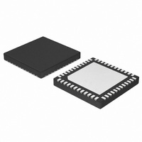
NCP4208MNR2G ON Semiconductor, NCP4208MNR2G Datasheet - Page 13

NCP4208MNR2G
Manufacturer Part Number
NCP4208MNR2G
Description
IC CTLR 8PH VR11.1 PMBUS 48-QFN
Manufacturer
ON Semiconductor
Datasheet
1.NCP4208MNR2G.pdf
(30 pages)
Specifications of NCP4208MNR2G
Applications
Controller, Intel VR11.1
Voltage - Input
4.7 ~ 5.75 V
Number Of Outputs
8
Voltage - Output
0.16 ~ 5 V
Operating Temperature
0°C ~ 85°C
Mounting Type
Surface Mount
Package / Case
48-TQFN Exposed Pad
Output Voltage
0.375 V to 1.6 V
Input Voltage
0.3 V to 6 V
Switching Frequency
1.5 MHz
Operating Temperature Range
0 C to + 85 C
Mounting Style
SMD/SMT
Duty Cycle (max)
100 %
Lead Free Status / RoHS Status
Lead free / RoHS Compliant
Available stocks
Company
Part Number
Manufacturer
Quantity
Price
Company:
Part Number:
NCP4208MNR2G
Manufacturer:
ON Semiconductor
Quantity:
1 200
Part Number:
NCP4208MNR2G
Manufacturer:
ON/安森美
Quantity:
20 000
control input voltage to the positive input is set via the VID
logic according to the voltages listed in Table 8. The VID
code is set using the VID Input pins or it can be programmed
over the I
NCP4208 outputs a voltage corresponding to the VID
Inputs. To output a voltage following the VOUT_Command
the user first needs to program the required VID Code. Then
the VID_EN Bits need to be enabled. The following is the
sequence:
positioning of the output voltage as a function of current,
commonly known as active voltage positioning. The output
of the amplifier is the COMP pin, which sets the termination
voltage for the internal PWM ramps.
with Resistor R
output voltage at this point. A current source (equal to I
from the FB pin flowing through R
no load offset voltage from the VID voltage. The no load
voltage is negative with respect to the VID DAC for Intel
CPU’s. The main loop compensation is incorporated into the
feedback network between FB and COMP.
the serial interface. This is done using Bits <5:0> of the
VOUT_CAL (0xDD) Command. The max offset that can be
applied is ±200 mV. The LSB size id 6.25 mV. A positive
offset is applied when Bit 5 = 0. A negative offset is applied
when Bit 5 = 1.
Dynamic VID
VID inputs while the controller is running. This allows the
output voltage to change while the supply is running and
supplying current to the load. This is commonly referred to
as Dynamic VID (DVID). A DVID can occur under either
light or heavy load conditions. The processor signals the
controller by changing the VID inputs (or by programming
a new VOUT_Command) in a single or multiple steps from
the start code to the finish code. This change can be positive
or negative.
change and ignores the DAC inputs for a minimum of 200 ns.
This time prevents a false code due to logic skew while the
VID inputs are changing. Additionally, the first VID change
initiates the PWRGD and CROWBAR blanking functions for
a minimum of 100 ms to prevent a false PWRGD or
Table 4. Offset Codes
This voltage is also offset by the droop voltage for active
The negative input (FB) is tied to the output sense location
An offset voltage can be added to the control voltage over
The NCP4208 has the ability to dynamically change the
When a VID bit changes state, the NCP4208 detects the
1. Program the required VID Code to the
2. Set the VID_EN bit (Bit 3) in the VR Config 1A
VOUT_Cal CODE
VOUT_Command code (0x21).
(0xD2) and on the VR Config 1B (0xD3).
2
0 0001
0 0010
0 0011
C using the VOUT_Command. By default, the
B
and is used for sensing and controlling the
OFFSET VOLTAGE
B
is used for setting the
+18.75 mV
+6.25 mV
+12.5 mV
http://onsemi.com
REF
)
13
CROWBAR event. Each VID change resets the internal
timer.
5 msec to ensure that the code is correct before initiating a
shutdown of the controller.
limit the DVID slew rates. These can be encountered when
the system does a large single VID step for power state
changes, thus the DVID slew rate needs to be limited to
prevent large inrush currents.
of the Ton_Transition (0xD6) command code. Table 5
provides the transition rate values.
Enhanced transient Mode
for both load step up and load release. For load step up it
senses the output of the error amp to determine if a load step
up has occurred and then sequences on the appropriate
number of phases to ramp up the output current.
and uses the load release information to trigger the TRDET
pin, which is then used to adjust the error amp feedback for
optimal positioning. This is especially important during
high frequency load steps.
ensure proper sequencing and balancing of phases during
high frequency load steps as well as minimizing the stress on
components such as the input filter and MOSFET’s.
Current Reference
This reference current sets I
programs the current based on the 1.8 V output.
Typically, R
Internal Delay Timer
an internal timer. The default time is 2 msec which can be
changed through the I
multiple delay timings (TD1, TD3, and TD5) during the
Table 5. Transition Rate Codes
If a VID off code is detected the NCP4208 will wait for
The NCP4208 also uses the TON_Transition (0xD6) to
The transition slew rate is programmed using Bits <2:0>
The NCP4208 incorporates enhanced transient response
For load release, it also senses the output of the error amp
Additional information is used during load transients to
The I
The delay times for the startup timing sequence are set by
Code
REF
000
001
010
100
101
011
110
111
pin is used to set an internal current reference.
IREF
is set to 121 kW to program I
I
REF
2
C interface. This timer is used for
+
Transition Rate (V/msec)
R
1.8 V
IREF
FB
. A resistor to ground
5 = default
13
15
11
1
3
7
9
REF
= 15 mA.
(eq. 8)


