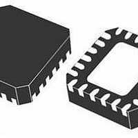
PM6641 STMicroelectronics, PM6641 Datasheet - Page 7

PM6641
Manufacturer Part Number
PM6641
Description
IC MONO VR DDR2/3 PC VFQFPN-48
Manufacturer
STMicroelectronics
Datasheet
1.PM6641TR.pdf
(47 pages)
Specifications of PM6641
Applications
Converter, DDR2, DDR3
Voltage - Input
2.7 ~ 5.5 V
Number Of Outputs
3
Voltage - Output
0.8 ~ 5.5 V
Operating Temperature
0°C ~ 85°C
Mounting Type
Surface Mount
Package / Case
48-VFQFN
Output Voltage
0.9 V
Output Current
3 A
Input Voltage
2.7 V to 5.5 V
Switching Frequency
1000 KHz
Operating Temperature Range
- 40 C to + 125 C
Mounting Style
SMD/SMT
For Use With
497-8425 - KIT EVAL PM6641 CHIPSET/DDR2/3
Lead Free Status / RoHS Status
Lead free / RoHS Compliant
Available stocks
Company
Part Number
Manufacturer
Quantity
Price
Company:
Part Number:
PM6641
Manufacturer:
BITECHNOL
Quantity:
2 000
Part Number:
PM6641
Manufacturer:
ST
Quantity:
20 000
Company:
Part Number:
PM6641TR
Manufacturer:
STM
Quantity:
35 839
PM6641
Table 2.
26
27
28
29
30
31
32
33
34
35
36
37
38
39
40
41
42
43
44
45
46
47
48
n°
COMP_1S5
SGND_1S5
SGND_1S5
VSW_1S5
VSW_1S5
SET_PH1
VFB_1S5
EN_1S05
VTTGND
VIN_1S5
EN_VTT
VTTREF
EN_1S5
EN_1S8
SS_1S5
VTTFB
LDOIN
DSCG
AGND
AGND
AVCC
VCC
VTT
Pin
Pin functions (continued)
Positive terminal of the external soft-start capacitor for 1.5 V rail.
See
Loop compensation output for 1.5 V rail.
loop on page 24
selection on page 38
Feedback input for 1.5 V rail.
See
Switcher power ground for 1.5 V rail.
Switcher power ground for 1.5 V rail.
Switch node for 1.5 V rail.
Switch node for 1.5 V rail.
Power supply input for 1.5 V rail.
Enable input for 1.05 V rail.
Enable input for 1.5 V rail.
Enable input for VTT rail. High in S0 system states. See
and S5 power management pins on page 22
Enable input for 1.8 V (VDDQ) rail. High in S0-S3 system states.
See
for details.
Analog and signal ground.
Switching regulator phase control.
See
Analog and signal ground.
Analog circuitry supply. Connect to +5 V by a simple RC filter.
LDO linear regulator power ground.
LDO linear regulator output. DDR2-3 termination voltage. See
Memory supply on page 20
buffered reference on page 21
LDO linear regulator input. Typically connected to the 1.8 V rail.
Reference voltage buffer output. See
page 20
page 21
Tracking/non-tracking discharge selection for DDR2-3 section. See
Chapter 7.7: Outputs soft-end on page 29
Feedback input for VTT linear regulator output.
+5 V switching circuitry supply. Bypass to AGND by a 100 nF capacitor.
Chapter 7.6: Outputs soft-start on page 28
Chapter 7.5: Output voltage divider on page 27
Chapter 7.1.4: S3 and S5 power management pins on page 22
Chapter 7.9: Phase management on page 30
Doc ID 13510 Rev 3
and
sections for details.
Chapter 7.1.2: VTT LDO and VTTREF buffered reference on
and
Chapter 8.4: SW regulator compensation components
sections for details.
and
sections for details.
Function
Chapter 7.1.2: VTT LDO and VTTREF
Chapter 7.1: Memory supply on
Chapter 7.3: SW regulators control
section for details.
section for details.
section for details.
section for details.
section for details
Chapter 7.1.4: S3
Pin settings
Chapter 7.1:
section
7/47


