PM6641 STMicroelectronics, PM6641 Datasheet - Page 37

PM6641
Manufacturer Part Number
PM6641
Description
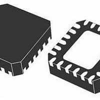
IC MONO VR DDR2/3 PC VFQFPN-48
Manufacturer
STMicroelectronics
Datasheet
1.PM6641TR.pdf
(47 pages)
Specifications of PM6641
Applications
Converter, DDR2, DDR3
Voltage - Input
2.7 ~ 5.5 V
Number Of Outputs
3
Voltage - Output
0.8 ~ 5.5 V
Operating Temperature
0°C ~ 85°C
Mounting Type
Surface Mount
Package / Case
48-VFQFN
Output Voltage
0.9 V
Output Current
3 A
Input Voltage
2.7 V to 5.5 V
Switching Frequency
1000 KHz
Operating Temperature Range
- 40 C to + 125 C
Mounting Style
SMD/SMT
For Use With
497-8425 - KIT EVAL PM6641 CHIPSET/DDR2/3
Lead Free Status / RoHS Status
Lead free / RoHS Compliant
Available stocks
Company
Part Number
Manufacturer
Quantity
Price
Company:
Part Number:
PM6641
Manufacturer:
BITECHNOL
Quantity:
2 000
Part Number:
PM6641
Manufacturer:
ST
Quantity:
20 000
Company:
Part Number:
PM6641TR
Manufacturer:
STM
Quantity:
35 839
PM6641
8.3
The losses due to the input capacitor are thus maximized when the duty-cycle is 0.5:
Equation 18
The input capacitor should be selected with a RMS rated current higher than I
Tantalum capacitors are good in term of low ESR and small size, but they occasionally can
burn out if subjected to very high current during operation. Multi-Layers-Ceramic-Capacitors
(MLCC) have usually a higher RMS current rating with smaller size and very low ESR.
When only one common input capacitor is chosen for the application, instead of one
dedicated capacitor for each regulator (close to each input power supply pins), the total
input current can be quite different from the arithmetic sum of the buck regulators RMS input
currents, if phase management is allowed (see
page 30
Output capacitor selection
Using tantalum or electrolytic capacitors, the selection is made referring to ESR and voltage
rating rather than by a specific capacitance value.
The output capacitor has to satisfy the output voltage ripple requirements. At a given
switching frequency, small inductor values are useful to reduce the size of the choke but
increase the inductor current ripple. Thus, to reduce the output voltage ripple a low ESR
capacitor is required:
Equation 19
where V
The zero introduced by the output capacitor ESR must be higher than the switching
frequency or must be compensated (see
page 24
Equation 20
In order to minimize the output voltage ripple, ceramic capacitors are suggested.
RIPPLE
section for details).
section for details):
is the maximum tolerable ripple voltage.
P
loss
=
ESR
Cin
Doc ID 13510 Rev 3
f
⋅
SW
I
2
CinRMS
ESR
>
f
Z
Chapter 7.3: SW regulators control loop on
=
≤
,
MAX
------------------------------------------- -
2π ESR C
V
RIPPLE
Δ
⋅
=
I
Chapter 7.9: Phase management on
, L
ESR
MAX
1
,
MAX
⋅
Cin
OUT
⋅
(
0
5 .
⋅
I
LOAD
,
Components selection
MAX
)
2
CinRMS,MAX
37/47
.


