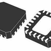
PM6641 STMicroelectronics, PM6641 Datasheet - Page 25

PM6641
Manufacturer Part Number
PM6641
Description
IC MONO VR DDR2/3 PC VFQFPN-48
Manufacturer
STMicroelectronics
Datasheet
1.PM6641TR.pdf
(47 pages)
Specifications of PM6641
Applications
Converter, DDR2, DDR3
Voltage - Input
2.7 ~ 5.5 V
Number Of Outputs
3
Voltage - Output
0.8 ~ 5.5 V
Operating Temperature
0°C ~ 85°C
Mounting Type
Surface Mount
Package / Case
48-VFQFN
Output Voltage
0.9 V
Output Current
3 A
Input Voltage
2.7 V to 5.5 V
Switching Frequency
1000 KHz
Operating Temperature Range
- 40 C to + 125 C
Mounting Style
SMD/SMT
For Use With
497-8425 - KIT EVAL PM6641 CHIPSET/DDR2/3
Lead Free Status / RoHS Status
Lead free / RoHS Compliant
Available stocks
Company
Part Number
Manufacturer
Quantity
Price
Company:
Part Number:
PM6641
Manufacturer:
BITECHNOL
Quantity:
2 000
Part Number:
PM6641
Manufacturer:
ST
Quantity:
20 000
Company:
Part Number:
PM6641TR
Manufacturer:
STM
Quantity:
35 839
PM6641
In order to obtain the typical integrative loop transfer function the signal stag e must
compensate for the power stage pole (due to the output capacitor and the load) and zero
(above the loop bandwidth if ceramic output capacitors are selected). The signal stage
transfer function is:
Equation 2
Where g
due to the output resistor divider (0.8 V / Vout). The external compensation network (R
and C
●
●
●
The control loop gain is obtained by multiplying G(s) by H(s):
Equation 3
This model provides good results if the control loop cut-off frequency f
fsw/10.
One zero, to compensate the power stage pole:
One pole in order to delete the static output voltage error;
One pole, if necessary, in order to compensate the high frequency zero due to the
output capacitor ESR:
RO
M
) introduces:
is the power stage transconductance, K
G
LOOP
(
) s
=
g
m
( G
K
L
) s
α
Doc ID 13510 Rev 3
=
sC
g
C
m
C
⎛
⎜
⎜
⎝
K
C
sC
R
L
C
(
sC
α
C
RO
Ro
sC
=
C
R
R
R
C
C
C
C
C
O
⎛
⎜ ⎜
⎝
=
+
sC
(
+
R
C
sC
C
1
C
O
Ro
O
)
Ro
C
R
L
C
+
R
R
ES
is a design parameter and α is the gain
R
+
C
C
ES
1
+
⎞
⎟
⎟
⎠
+
)
C
⋅
1
C
sC
Ro
C
(
O
sC
+
(
R
1
⎞
⎟ ⎟
⎠
O
ES
R
ES
+
R
CO
+
O
1
Device description
)
)
is lower than about
+
1
R
O
c
25/47
, C
c


