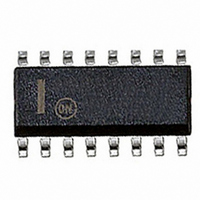
MC33023DWR2G ON Semiconductor, MC33023DWR2G Datasheet - Page 12

MC33023DWR2G
Manufacturer Part Number
MC33023DWR2G
Description
IC CTRLR PWM HS SGL ENDED 16SOIC
Manufacturer
ON Semiconductor
Datasheet
1.MC33023DWR2G.pdf
(18 pages)
Specifications of MC33023DWR2G
Pwm Type
Voltage/Current Mode
Number Of Outputs
1
Frequency - Max
1MHz
Duty Cycle
90%
Voltage - Supply
10 V ~ 30 V
Buck
No
Boost
No
Flyback
No
Inverting
No
Doubler
No
Divider
No
Cuk
No
Isolated
Yes
Operating Temperature
-40°C ~ 105°C
Package / Case
16-SOIC (0.300", 7.5mm Width)
Frequency-max
1MHz
Duty Cycle (max)
90 %
Output Voltage
5.05 V to 5.15 V
Output Current
500 mA
Mounting Style
SMD/SMT
Switching Frequency
1000 KHz
Operating Supply Voltage
30 V
Maximum Operating Temperature
+ 105 C
Fall Time
30 ns
Minimum Operating Temperature
- 40 C
Rise Time
30 ns
Synchronous Pin
Yes
Topology
Flyback, Forward
Number Of Pwm Outputs
1
On/off Pin
Yes
Adjustable Output
No
Switching Freq
1MHz
Operating Supply Voltage (max)
30V
Operating Temperature Classification
Industrial
Mounting
Surface Mount
Pin Count
16
Package Type
SOIC W
Lead Free Status / RoHS Status
Lead free / RoHS Compliant
Other names
MC33023DWR2GOS
Available stocks
Company
Part Number
Manufacturer
Quantity
Price
slope necessary. By choosing R
R
by I
leading edge spike on the current waveform. This sense signal can also
be used at the ramp input pin for current mode control. For ramp
compensation it is necessary to know the gain of the current feedback
loop. If a transformer is used, the gain can be calculated by:
M
When only one output is used, this method of slope compensation can be used and it is relatively noise immune. Resistor R
Output
M
The addition of an RC filter will eliminate instability caused by the
can be adjusted to achieve the required slope. The diode provides a reset pulse at the ramp input at the end of every cycle. The charge current I
= C
M
S
Figure 24. Resistive Current Sensing
e
R
. Then R
M
C
Current Sense
M
Transformer
M
can be calculated by R
R
C
R
w
A
f
f
i
+
M
and C
turns ratio
9
Ramp
R Sense
Input
7
3
M
with a larger time constant than the switching frequency, you can assume that its charge is linear. First choose C
is noise sensitive. Capacitor C
signal is added to the current signal by a voltage divider consisting of
resistors R
Figure 26A. Slope Compensation (Noise Sensitive)
1.25 V
Current Sense
This method of slope compensation is easy to implement, however, it
Figure 26B. Slope Compensation (Noise Immune)
M
= V
Information
CC
1
/I
M.
and R
C
T
I
Sense
2
.
R
2
R
http://onsemi.com
1
C
Figure 26.
1
4
5
6
7
3
1
provides AC coupling. The oscillator
12
leading edge spike on the current waveform. This sense signal can also
be used at the ramp input pin for current mode control. For ramp
compensation it is necessary to know the gain of the current feedback
loop. The gain can be calculated by:
1.25 V
The addition of an RC filter will eliminate instability caused by the
Current Sense
Figure 25. Primary Side Current Sensing
Oscillator
Resistor
R
f
C
A
M
Output
i
+
9
R
C
M
turns ratio
f
M
R
Ramp
and capacitor C
w
Input
7
3
R
1.25 V
w
M
M
provide the added
can be calculated
I
Sense
M
, then


