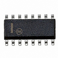
MC33023DWR2G ON Semiconductor, MC33023DWR2G Datasheet - Page 10

MC33023DWR2G
Manufacturer Part Number
MC33023DWR2G
Description
IC CTRLR PWM HS SGL ENDED 16SOIC
Manufacturer
ON Semiconductor
Datasheet
1.MC33023DWR2G.pdf
(18 pages)
Specifications of MC33023DWR2G
Pwm Type
Voltage/Current Mode
Number Of Outputs
1
Frequency - Max
1MHz
Duty Cycle
90%
Voltage - Supply
10 V ~ 30 V
Buck
No
Boost
No
Flyback
No
Inverting
No
Doubler
No
Divider
No
Cuk
No
Isolated
Yes
Operating Temperature
-40°C ~ 105°C
Package / Case
16-SOIC (0.300", 7.5mm Width)
Frequency-max
1MHz
Duty Cycle (max)
90 %
Output Voltage
5.05 V to 5.15 V
Output Current
500 mA
Mounting Style
SMD/SMT
Switching Frequency
1000 KHz
Operating Supply Voltage
30 V
Maximum Operating Temperature
+ 105 C
Fall Time
30 ns
Minimum Operating Temperature
- 40 C
Rise Time
30 ns
Synchronous Pin
Yes
Topology
Flyback, Forward
Number Of Pwm Outputs
1
On/off Pin
Yes
Adjustable Output
No
Switching Freq
1MHz
Operating Supply Voltage (max)
30V
Operating Temperature Classification
Industrial
Mounting
Surface Mount
Pin Count
16
Package Type
SOIC W
Lead Free Status / RoHS Status
Lead free / RoHS Compliant
Other names
MC33023DWR2GOS
Available stocks
Company
Part Number
Manufacturer
Quantity
Price
current limit comparator. This can be accomplished by
biasing pin 11 to a level greater than 1.4 V but less than 3.0 V.
Under these conditions, the shutdown comparator and
soft−start latch are activated during an overcurrent event
causing the converter to enter an hiccup mode.
Undervoltage Lockout
The first senses V
V
the outputs can be enabled and the Soft−Start latch released.
If V
are disabled and the Soft−Start latch is activated. When the
UVLO is active, the part is in a low current standby mode
allowing the IC to have an off−line bootstrap startup circuit.
Typical startup current is 500 mA.
Output
specifically designed for direct drive of power MOSFETs.
It is capable of up to ± 2.0 A peak drive current with a typical
rise and fall time of 30 ns driving a 1.0 nF load.
With proper implementation, a significant reduction of
switching transient noise imposed on the control circuitry is
possible. The separate V
designer added flexibility in tailoring the drive voltage
independent of V
Reference
to an initial accuracy of ±1.0% at 25°C. This reference has
short circuit protection and can source in excess of 10 mA
for powering additional control system circuitry.
Design Considerations
wire−wrap or plug−in prototype boards. With high
frequency, high power, switching power supplies it is
imperative to have separate current loops for the signal paths
and for the power paths. The printed circuit layout should
contain a ground plane with low current signal and high
current switch and output grounds returning on separate
paths back to the input filter capacitor. Shown in Figure 36
is a printed circuit layout of the application circuit. Note how
the power and ground traces are run. All bypass capacitors
CC
In certain applications, it may be desirable to disable the
There are two undervoltage lockout circuits within the IC.
The MC34023 has a high current totem pole output
Separate pins for V
A 5.1 V bandgap reference is pinned out and is trimmed
Do not attempt to construct the converter on
CC
must exceed 9.2 V and V
falls below 8.4 V or V
CC
CC
I shutdown +
.
and the second V
C
and Power Ground are provided.
C
ref
supply input also allows the
ref
falls below 3.6 V, the outputs
R Sense
1.4 V
must exceed 4.2 V before
ref
. During power−up,
http://onsemi.com
10
and snubbers should be connected as close as possible to the
specific part in question. The PC board lead lengths must be
less than 0.5 inches for effective bypassing for snubbing.
Instabilities
at any given duty cycle. The instability is caused by the
current feedback loop. It has been shown that the instability
is caused by a double pole at half the switching frequency.
If an external ramp (S
of the current−sense waveform, stability can be achieved.
compensation. If too much is added the system will start to
perform like a voltage mode regulator. All benefits of
current mode control will be lost. Figure 26 is an example of
one way in which external ramp compensation can be
implemented.
external ramp slope necessary to add that will achieve
stability in the current loop. For the following equations, the
calculated values for the application circuit in Figure 35 are
also shown.
where:
For the application circuit: S e +
In current mode control, an instability can be encountered
One must be careful not to add too much ramp
Compensation S
A simple equation can be used to calculate the amount of
Ramp
N
P
Figure 21. Ramp Compensation
, N
V
R
e
A
O
S
L
S
i
S e +
= DC output voltage
= number of power transformer primary
=
= gain of the current sense network
=
= output inductor
= current sense resistance
or secondary turns
(see Figures 24 and 25)
Ramp Input
Signal S
Current
e
) is added to the on−time ramp (S
V O
L
Ramp Compensation
n
N S
N P
= 0.115 V/ms
(R S )A
1.8 μ
5
1.25 V
i
2
8
( 0.3 )( 0.55 )
n
)


