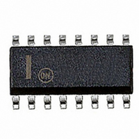
NCP1396BDR2G ON Semiconductor, NCP1396BDR2G Datasheet - Page 16

NCP1396BDR2G
Manufacturer Part Number
NCP1396BDR2G
Description
IC CTRLR OVP HV 16SOIC
Manufacturer
ON Semiconductor
Type
High Performance Resonant Mode Controllersr
Datasheet
1.NCP1396BDR2G.pdf
(25 pages)
Specifications of NCP1396BDR2G
Pwm Type
Voltage Mode
Number Of Outputs
1
Frequency - Max
575kHz
Duty Cycle
52%
Voltage - Supply
10.5 V ~ 20 V
Buck
No
Boost
No
Flyback
No
Inverting
No
Doubler
No
Divider
No
Cuk
No
Isolated
Yes
Operating Temperature
-40°C ~ 125°C
Package / Case
16-SOIC (3.9mm Width, 15 Leads)
Frequency-max
575kHz
Output Voltage Range
20 V
Output Current
300 uA
Power Dissipation
42 mW
Operating Temperature Range
- 40 C to + 125 C
Mounting Style
SMD/SMT
Input Voltage
12V
Frequency
500kHz
Supply Voltage Range
20V
Digital Ic Case Style
SOIC
No. Of Pins
16
Svhc
No SVHC (15-Dec-2010)
Base Number
1396
Rohs Compliant
Yes
Lead Free Status / RoHS Status
Lead free / RoHS Compliant
Other names
NCP1396BDR2GOS
NCP1396BDR2GOS
NCP1396BDR2GOSTR
NCP1396BDR2GOS
NCP1396BDR2GOSTR
Available stocks
Company
Part Number
Manufacturer
Quantity
Price
Company:
Part Number:
NCP1396BDR2G
Manufacturer:
ON Semiconductor
Quantity:
313
2000
1900
1800
1700
1600
1500
1400
1300
1200
1100
1000
Figure 36. Minimum Switching Frequency Resistor
Figure 37. Minimum Switching Frequency Resistor
500
450
400
350
300
250
200
150
100
100
900
800
700
600
500
400
300
200
100
90
80
70
60
50
40
30
20
1
10
3.5
Figure 38. Dead- -Time Resistor Selection
Selection (Fmin = 100 kHz to 500 kHz)
Selection (Fmin = 20 kHz to 100 kHz)
13.5
15
3
20
23.5
25
RFmin (kΩ)
RFmin (kΩ)
33.5
Rdt (kΩ)
5
30
43.5
35
7
53.5
40
63.5
V
FB = 1 V
DT = 300 ns
V
FB = 1 V
DT = 300 ns
45
Vcc = 12 V
CC
CC
9
= 12 V
= 12 V
73.5 83.5
50
http://onsemi.com
11
55
16
ORing Capability
frequency variation linked to an event appearance (instead
of abruptly stopping pulses), then the FB pin lends itself
very well to the addition of other sweeping loops. Several
diodes can easily be used perform the job in case of reaction
to a fault event or to regulate on the output current (CC
operation). Figure 39 shows how to do it.
Dead- -time Control
half- - bridge configuration comes to play. The dead- - time
technique consists in inserting a period during which both
high and low side switches are off. Of course, the
dead- - time amount differs depending on the switching
frequency, hence the ability to adjust it on this controller.
The option ranges between 100 ns and 2 ms. The dead- - time
is actually made by controlling the oscillator discharge
current. Figure 40 portrays a simplified VCO circuit based
on Figure 31.
If for any particular reason, there is a need for a
Dead- - time control is an absolute necessity when the
Figure 39. Thanks to the FB Configuration, Loop
In1
In2
ORing is Easy to Implement
V
CC
FB
20 k
VCO


