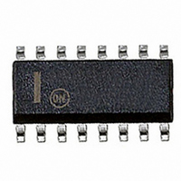
NCP1396BDR2G ON Semiconductor, NCP1396BDR2G Datasheet - Page 14

NCP1396BDR2G
Manufacturer Part Number
NCP1396BDR2G
Description
IC CTRLR OVP HV 16SOIC
Manufacturer
ON Semiconductor
Type
High Performance Resonant Mode Controllersr
Datasheet
1.NCP1396BDR2G.pdf
(25 pages)
Specifications of NCP1396BDR2G
Pwm Type
Voltage Mode
Number Of Outputs
1
Frequency - Max
575kHz
Duty Cycle
52%
Voltage - Supply
10.5 V ~ 20 V
Buck
No
Boost
No
Flyback
No
Inverting
No
Doubler
No
Divider
No
Cuk
No
Isolated
Yes
Operating Temperature
-40°C ~ 125°C
Package / Case
16-SOIC (3.9mm Width, 15 Leads)
Frequency-max
575kHz
Output Voltage Range
20 V
Output Current
300 uA
Power Dissipation
42 mW
Operating Temperature Range
- 40 C to + 125 C
Mounting Style
SMD/SMT
Input Voltage
12V
Frequency
500kHz
Supply Voltage Range
20V
Digital Ic Case Style
SOIC
No. Of Pins
16
Svhc
No SVHC (15-Dec-2010)
Base Number
1396
Rohs Compliant
Yes
Lead Free Status / RoHS Status
Lead free / RoHS Compliant
Other names
NCP1396BDR2GOS
NCP1396BDR2GOS
NCP1396BDR2GOSTR
NCP1396BDR2GOS
NCP1396BDR2GOSTR
Available stocks
Company
Part Number
Manufacturer
Quantity
Price
Company:
Part Number:
NCP1396BDR2G
Manufacturer:
ON Semiconductor
Quantity:
313
frequency and the minimum switching frequency. In LLC
configurations, for circuits working above the resonant
frequency, a high precision is required on the minimum
frequency, hence the 3% specification. This minimum
switching frequency is actually reached when no feedback
closes the loop. It can happen during the startup sequence,
a strong output transient loading or in a short- - circuit
condition. By installing a resistor from pin 4 to GND, the
minimum frequency is set. Using the same philosophy,
The designer needs to program the maximum switching
2. The A version does not activate the soft- - start
products where the designer can use an external
startup resistor, whereas the B is more
recommended for industrial / medical
applications where a 12 V auxiliary supply
directly powers the chip.
upon release of the fast fault input. This is to let
the designer implement skip cycle. To the
opposite, the B version goes back to operation
upon the fast fault pin release via a soft- - start
sequence.
V
CC
Rt sets
Fmin for V(FB) = 0
Rdt sets
the dead- -time
Fmax sets
the maximum Fsw
Fmax
DT
Rt
FB
Rfb
20 k
Figure 31. The Simplified VCO Architecture
Vref
Vref
Vdd
Vdd
Vdd
http://onsemi.com
Imin
Imin
Cint
0 to I_Fmax
IDT
14
Voltage- -Controlled Oscillator
allowing operation from 100 kHz up to 1 MHz. However,
as a division by two internally creates the two Q and Q
outputs, the final effective signal on output Mlower and
Mupper switches between 50 kHz and 500 kHz. The VCO
is configured in such a way that if the feedback pin goes up,
the switching frequency also goes up. Figure 31 shows the
architecture of this oscillator.
wiring a resistor from pin 2 to GND will set the maximum
frequency excursion. To improve the circuit protection
features, we have purposely created a dead zone, where the
feedback loop has no action. This is typically below 1.2 V.
Figure 32 details the arrangement where the internal
voltage (that drives the VCO) varies between 0 and 2.3 V.
However, to create this swing, the feedback pin (to which
the optocoupler emitter connects), will need to swing
typically between 1.2 V and 5.3 V.
The VCO section features a high- - speed circuitry
FBinternal
+
+
- -
+
- -
max
max
Fsw
Vb_off
+
+
- -
D
Clk
S
R
Q
Q
Vfb < Vb_off
Start fault timer
A
B


