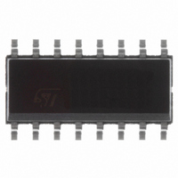
L5993D STMicroelectronics, L5993D Datasheet - Page 13

L5993D
Manufacturer Part Number
L5993D
Description
IC PWM CONTROLLER 16 SOIC
Manufacturer
STMicroelectronics
Datasheet
1.L5993D.pdf
(22 pages)
Specifications of L5993D
Pwm Type
Current Mode
Number Of Outputs
1
Frequency - Max
1MHz
Duty Cycle
85%
Voltage - Supply
11 V ~ 20 V
Buck
No
Boost
No
Flyback
Yes
Inverting
No
Doubler
No
Divider
No
Cuk
No
Isolated
Yes
Operating Temperature
0°C ~ 105°C
Package / Case
16-SOIC (3.9mm Width)
Frequency-max
1MHz
Lead Free Status / RoHS Status
Contains lead / Request inventory verification
Other names
497-2387-5
Available stocks
Company
Part Number
Manufacturer
Quantity
Price
Figure 29. Half duty cycle option.
Figure 30. Constant Power circuit internal schematic
Pin 16. C-POWER (Constant Power Function).
An external capacitor connected between this pin
and SGND completes the peak-holding circuit that
detects the peak voltage of the synchronized os-
cillator. The circuit gets a DC voltage (which de-
creases as the synchronizing frequency fed into
pin 1 (SYNC) rises) used to clamp the error ampli-
fier output (V
nal schematic of fig. 30.
In this way the pulse-by-pulse setpoint is moved
downwards as the frequency rises (and vice versa for
a frequency decrease, due to the 47k discharge re-
sistor) and, as a result, the maximum power deliver-
ableto the load is held roughly constant.
The external capacitor must be large enough to
get a real DC voltage on the pin. Considering the
spread of the internal 47k
capacitance value (C
1% ripple superimposed on the DC voltage is:
COMP
C
), as shown in the detailed inter-
CP
CP
C-POWER
330
) needed to have less than
C T
R
T
VREF
RCT
C CP
1
resistor, the minimum
V15=GND
V5=V13=GND
V15=VREF
V5=V13=GND
mi n
4
16
2
5
2.5V
VFB
,
t c
t c
BUFFER
+
+
-
-
E/A
CLAMP
D97IN768A
COMP
6
D1
t
d
t
d
47K
Q1
D2
Q2
D97IN498
where
quency.
When this function is not used, pin 16 has to be
connecteddirectly to pin 4.
Considering the ordinary design criteria for the
transformer, the circuit usually works well without
any adjustment. Anyway, the variations of the
maximum power limit on varying the switching fre-
quency and/or the mains voltage can be mini-
mized by modifying one or more of the following
parameters:
- Primary inductance;
- Transformer turns ratio;
- Oscillator free-running frequency;
- Sense resistor.
A trial process is required, involving the parame-
ters that are more practicable to modify. In fact,
the optimum behavior is achieved for a specific
combination of the above parameters and de-
30K
30K
TIMING
SYNC
min
V10
V10
15K
1
V2
V2
1V
(Hz) is the minimum synchronizing fre-
D
D
X
X
=
=
2 ·t c + t d
t c + t d
t c
t c
ISEN
COMPARATOR
+
-
13
PWM
L5993
TO PWM
LATCH
L5993
13/22


