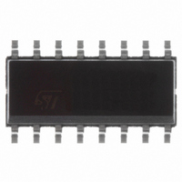
L5993D STMicroelectronics, L5993D Datasheet

L5993D
Specifications of L5993D
Available stocks
Related parts for L5993D
L5993D Summary of contents
Page 1
... SMPS. SYNC DC-LIM TIMING 25V + T 15V/10V - PWM UVLO BLANKING PWM VREF OK CLK FAULT DIS SOFT-START SGND COMP L5993 SO16N L5993D (SO16) VREF 4 Vref 13V 10 OUT 11 PGND + 2.5V 5 E/A - VFB D97IN765 1/22 ...
Page 2
L5993 ABSOLUTE MAXIMUM RATINGS Symbol V Supply Voltage (I < 50mA) (*) Output Peak Pulse Current OUT Analog Inputs & Outputs (6,7) Analog Inputs & Outputs (1,2,3,4,5,15,14, 13, 16) P Power Dissipation @ T tot @ T ...
Page 3
ELECTRICAL CHARACTERISTICS (V unless otherwise specified.) Symbol Parameter REFERENCE SECTION V Output Voltage Ref Line Regulation Load Regulation T Temperature Stability S Total Variation I Short Circuit Current OS Power Down/UVLO OSCILLATOR SECTION Initial Accuracy Duty Cycle Duty Cycle Duty ...
Page 4
L5993 ELECTRICAL CHARACTERISTICS (continued.) Symbol Parameter OUTPUT SECTION Collector Leakage Fall Time Rise Time UVLO Saturation SUPPLY SECTION V Startup voltage CCON V Minimum Operating Voltage CCOFF V ULVO Hysteresis hys I Start Up Current S I Operating Current op ...
Page 5
Figure 3. Quiescent current vs. input voltage ...
Page 6
L5993 Figure 9. Vref SVRR vs. switching frequency. SVRR (dB) 120 100 1000 fsw (Hz) Figure 11. Output saturation ...
Page 7
Figure 15. Switching frequency vs. temperature. fsw (KHz) 320 Rt= 4.5Kohm 1nF 310 Vcc = 15V, V15= 0 300 290 280 -50 - Figure 17. Maximum Duty Cycle vs Vpin3. DC ...
Page 8
L5993 CONSTANT POWER FUNCTION Pulse-by-pulse current limitation prevents peak primary current from exceeding a given level. This, in turn, limits the maximum power deliver- able to the output or, in other words, the power capability of a converter. The capability, ...
Page 9
Figure 21. Oscillator and synchronization internal schematic REF CLAMP RCT ered at pin 1 and defines the upper extreme of the duty cycle range, D (see pin 15 for D ...
Page 10
L5993 Pin 5. VFB (Error Amplifier Inverting Input). The feedback signal is applied to this pin and is com- pared to the E/A internal reference (2.5V). The E/A output generates the control voltage which fixes the duty cycle. The E/A ...
Page 11
T 4.5 C hic SSC SSD Since the system tries restarting each hiccup cy- cle, there is not any ...
Page 12
L5993 Figure 27. Internal LEB ISEN 1.2V Pin 12. SGND (Signal Ground). This ground refer- ences the control circuitry of the IC, so all the ground connections of the external parts related to control functions must lead ...
Page 13
Figure 29. Half duty cycle option. V15=GND V5=V13=GND t c V15=VREF V5=V13=GND t c Figure 30. Constant Power circuit internal schematic VFB 5 2.5V VREF C-POWER RCT C T Pin 16. C-POWER (Constant ...
Page 14
L5993 pends both on the mains voltage range and the synchronization frequency range. An additional ”fine tuning” can be achieved by adding a small DC offset (in the ten mV) on the current sense pin (13, ISEN). For wide range ...
Page 15
APPLICATION IDEAS Here follows a series of ideas/suggestions aimed at Figure 31. Typical application circuit for 15” Multisync monitor (70W) either improving performance or solving common application problems of L5993 based supplies. L5993 15/22 ...
Page 16
L5993 Figure 32. Isolated MOSFET Drive & Current Transformer Sensing in 2-switch Topologies L5993 12 11 PGND SGND Figure 33. Low consumption start-up 2.2M 20V 47K D97IN770B Figure 34. Bipolar Transistor Drive L5993 16/22 ISOLATION BOUNDARY 10 ...
Page 17
Figure 35. Typical E/A compensation networks. From Error Amp compensation circuit for stabilizing any current-mode topology except for boost and flyback converters operating with continuous inductor current. From ...
Page 18
L5993 Figure 38. Protection against overvoltage/feedback disconnection (latched) R START DIS L5993 SGND PGND D97IN774 Figure 39. Protection against overvol- tage/feedback disconnection (not latched) R START V CC VREF 4 8 L5993 DC 3 ...
Page 19
Figure 43. Device shutdown on mains undervoltage 400V DC 5.1 Figure 44. Constant power ”Fine Tuning”. Figure 45. Synchronization to flyback pulses (for monitors). Figure 46. Switching frequency halving on absence of sync. signal (for monitor). f ...
Page 20
L5993 mm DIM. MIN. TYP. MAX. MIN. a1 0.51 0.020 B 0.77 1.65 0.030 b 0 8.5 e 2.54 e3 17.78 F 7.1 I 5.1 L 3.3 Z 1.27 20/22 inch OUTLINE AND MECHANICAL DATA ...
Page 21
DIM. MIN. TYP. MAX. MIN. A 1.75 a1 0.1 0.25 0.004 a2 1.6 b 0.35 0.46 0.014 b1 0.19 0.25 0.007 C 0 (typ.) D (1) 9.8 10 0.386 E 5.8 6.2 0.228 e 1.27 e3 8.89 ...
Page 22
... STMicroelectronics. Specification mentioned in this publication are subject to change without notice. This publication supersedes and replaces all information previously supplied. STMicroelectronics products are not authorized for use as critical components in life support devices or systems without express written approval of STMicroelectronics. The ST logo is a registered trademark of STMicroelectronics 1999 STMicroelectronics – ...


