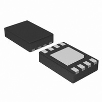
SE98ATP,147 NXP Semiconductors, SE98ATP,147 Datasheet - Page 6

SE98ATP,147
Manufacturer Part Number
SE98ATP,147
Description
IC TEMPERATURE SENSOR DDR 8HWSON
Manufacturer
NXP Semiconductors
Datasheet
1.SE98ATP547.pdf
(43 pages)
Specifications of SE98ATP,147
Function
Temp Monitoring System (Sensor)
Topology
ADC (Sigma Delta), Register Bank
Sensor Type
Internal
Sensing Temperature
-40°C ~ 125°C
Output Type
I²C™/SMBus™
Output Alarm
Yes
Output Fan
Yes
Voltage - Supply
1.7 V ~ 3.6 V
Operating Temperature
-40°C ~ 125°C
Mounting Type
Surface Mount
Package / Case
8-WSON
Full Temp Accuracy
+/- 2 C
Digital Output - Bus Interface
2-Wire
Digital Output - Number Of Bits
11
Supply Voltage (max)
3.6 V
Supply Voltage (min)
1.7 V
Maximum Operating Temperature
+ 125 C
Minimum Operating Temperature
- 40 C
Supply Current
250 uA
Lead Free Status / RoHS Status
Lead free / RoHS Compliant
NXP Semiconductors
SE98A_4
Product data sheet
7.3.1 EVENT pin output voltage levels and resistor sizing
7.3 EVENT output condition
The EVENT output indicates conditions such as the temperature crossing a predefined
boundary. The EVENT modes are very configurable and selected using the configuration
register (CONFIG). The interrupt mode or comparator mode is selected using CONFIG[0],
using either TCRIT/UPPER/LOWER or TCRIT only temperature bands (CONFIG[2]) as
modified by hysteresis (CONFIG[10:9]). The UPPER/LOWER (CONFIG[6]) and TCRIT
(CONFIG[7]) bands can be locked.
temperature versus time, with the corresponding behavior of the EVENT output in each of
these modes.
Upon device power-up, the default condition for the EVENT output is high-impedance to
prevent spurious or unwanted alarms, but can be later enabled (CONFIG[3]). EVENT
output polarity can be set to active HIGH or active LOW (CONFIG[1]). EVENT status can
be read (CONFIG[4]) and cleared (CONFIG[5]).
If the device enters Shutdown mode (CONFIG[8]) with asserted EVENT output, the output
remains asserted during shutdown.
The EVENT open-drain output is typically pulled up to a voltage level from 0.9 V to 3.6 V
with an external pull-up resistor, but there is no real lower limit on the pull-up voltage for
the EVENT pin since it is simply an open-drain output. It could be pulled up to 0.1 V and
would not affect the output. From the system perspective, there will be a practical limit.
That limit will be the voltage necessary for the device monitoring the interrupt pin to detect
a HIGH on its input. A possible practical limit for a CMOS input would be 0.4 V. Another
thing to consider is the value of the pull-up resistor. When a low supply voltage is applied
to the drain (through the pull-up resistor) it is important to use a higher value pull-up
resistor, to allow a larger maximum signal swing on the EVENT pin.
•
Advisory notification:
– NXP device: After power-up, bit 3 (1) and bit 2 or bit 0 (leave as 0 or 1) can be set
– Competitor device: Does not require that bit 3 be cleared (e.g., set back to (0))
– Work-around: In order to change bit 2 or bit 0 once bit 3 (1) is set, bit 3 (0) must be
– SE98B will allow bit 2 or bit 0 to be changed even if bit 3 is set.
at the same time (e.g., in same byte) but once bit 3 is set (1) then changing bit 2 or
bit 0 has no effect on the device operation.
before changing bit 2 or bit 0.
cleared in one byte and then change bit 2 or bit 0 and reset bit 3 (1) in the next
byte.
Rev. 04 — 25 November 2009
Figure 6
DDR memory module temp sensor, 1.7 V to 3.6 V
shows an example of the measured
© NXP B.V. 2009. All rights reserved.
SE98A
6 of 43


