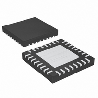
MAX1533AETJ+ Maxim Integrated Products, MAX1533AETJ+ Datasheet - Page 28

MAX1533AETJ+
Manufacturer Part Number
MAX1533AETJ+
Description
IC POWER SUPPLY CONTROLER 32TQFN
Manufacturer
Maxim Integrated Products
Datasheet
1.MAX1533AETJT.pdf
(38 pages)
Specifications of MAX1533AETJ+
Applications
Power Supply Controller
Voltage - Input
4.5 ~ 26 V
Current - Supply
15µA
Operating Temperature
-40°C ~ 85°C
Mounting Type
Surface Mount
Package / Case
32-TQFN Exposed Pad
Lead Free Status / RoHS Status
Lead free / RoHS Compliant
Voltage - Supply
-
Lead Free Status / Rohs Status
Lead free / RoHS Compliant
High-Efficiency, 5x Output, Main Power-Supply
Controllers for Notebook Computers
• Maximum Load Current. There are two values to
• Switching Frequency. This choice determines the
• Inductor Operating Point. This choice provides
The switching frequency and inductor operating point
determine the inductor value as follows:
For example: I
f
Find a low-loss inductor with the lowest possible DC
resistance that fits in the allotted dimensions. Most
inductor manufacturers provide inductors in standard
values, such as 1.0µH, 1.5µH, 2.2µH, 3.3µH, etc. Also
28
OSC
consider. The peak load current (I
mines the instantaneous component stresses and fil-
tering requirements and thus drives output-capacitor
selection, inductor saturation rating, and the design
of the current-limit circuit. The continuous load cur-
rent (I
thus drives the selection of input capacitors,
MOSFETs, and other critical heat-contributing com-
ponents.
basic trade-off between size and efficiency. The opti-
mal frequency is largely a function of maximum input
voltage, due to MOSFET switching losses that are
proportional to frequency and V
quency is also a moving target, due to rapid improve-
ments in MOSFET technology that are making higher
frequencies more practical.
trade-offs between size vs. efficiency and transient
response vs. output ripple. Low inductor values pro-
vide better transient response and smaller physical
size, but also result in lower efficiency and higher
output ripple due to increased ripple currents. The
minimum practical inductor value is one that causes
the circuit to operate at the edge of critical conduc-
tion (where the inductor current just touches zero
with every cycle at maximum load). Inductor values
lower than this grant no further size-reduction bene-
fit. The optimum operating point is usually found
between 20% and 50% ripple current. When pulse
skipping (SKIP low and light loads), the inductor
value also determines the load-current value at
which PFM/PWM switchover occurs.
______________________________________________________________________________________
= 300kHz, 30% ripple current or LIR = 0.3.
L
=
LOAD
L
12V
=
LOAD(MAX)
) determines the thermal stresses and
V f
×
IN OSC LOAD(MAX)
V
5
300kHz
OUT
V
×
(
12
(
I
V
= 5A, V
V
IN
×
- 5V
- V
5
A
Inductor Selection
)
OUT
IN
×
IN
2
= 12V, V
LIR
)
0 3
. The optimum fre-
LOAD(MAX)
.
=
6 50
.
OUT
μ
) deter-
H
= 5V,
look for nonstandard values, which can provide a better
compromise in LIR across the input voltage range. If
using a swinging inductor (where the no-load induc-
tance decreases linearly with increasing current), evalu-
ate the LIR with properly scaled inductance values. For
the selected inductance value, the actual peak-to-peak
inductor ripple current (ΔI
Ferrite cores are often the best choice, although pow-
dered iron is inexpensive and can work well at 200kHz.
The core must be large enough not to saturate at the
peak inductor current (I
A coupled inductor or transformer can be substituted
for the inductor in the 5V SMPS to create an auxiliary
output (Figure 1). The MAX1537A is particularly well
suited for such applications because the secondary
feedback threshold automatically triggers DL5 even if
the 5V output is lightly loaded.
The power requirements of the auxiliary supply must be
considered in the design of the main output. The trans-
former must be designed to deliver the required current
in both the primary and the secondary outputs with the
proper turns ratio and inductance. The power ratings of
the synchronous-rectifier MOSFETs and the current limit
in the MAX1537A must also be adjusted accordingly.
Extremes of low input-output differentials, widely different
output loading levels, and high turns ratios can further
complicate the design due to parasitic transformer para-
meters such as interwinding capacitance, secondary
resistance, and leakage inductance. Power from the
main and secondary outputs is combined to get an
equivalent current referred to the main output. Use this
total current to determine the current limit (see the
Setting the Current Limit section):
where P
outputs and I
used to determine the primary inductance (see the
Inductor Selection section).
(For the MAX1537A Auxiliary Output)
TOTAL
ΔI
I
INDUCTOR
PEAK
I
LOAD(MAX)
LOAD(MAX)
is the sum of the main and secondary
=
I
LOAD MAX
=
PEAK
(
V
= P
is the maximum output current
INDUCTOR
OUT
TOTAL
):
V
)
IN OSC
Transformer Design
+
(
V
Δ
IN
f
I
INDUCTOR
/ V
) is defined by:
-
2
OUT5
V
L
OUT
)


