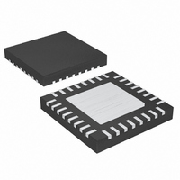
MAX1533AETJ+ Maxim Integrated Products, MAX1533AETJ+ Datasheet - Page 14

MAX1533AETJ+
Manufacturer Part Number
MAX1533AETJ+
Description
IC POWER SUPPLY CONTROLER 32TQFN
Manufacturer
Maxim Integrated Products
Datasheet
1.MAX1533AETJT.pdf
(38 pages)
Specifications of MAX1533AETJ+
Applications
Power Supply Controller
Voltage - Input
4.5 ~ 26 V
Current - Supply
15µA
Operating Temperature
-40°C ~ 85°C
Mounting Type
Surface Mount
Package / Case
32-TQFN Exposed Pad
Lead Free Status / RoHS Status
Lead free / RoHS Compliant
Voltage - Supply
-
Lead Free Status / Rohs Status
Lead free / RoHS Compliant
High-Efficiency, 5x Output, Main Power-Supply
Controllers for Notebook Computers
14
MAX1533A
______________________________________________________________________________________
10
11
12
13
14
15
16
17
18
19
20
21
22
23
24
PIN
MAX1537A
12
13
14
15
16
17
18
19
20
21
22
23
24
25
26
PGOOD
NAME
PGND
CSH3
LDO3
LDO5
BST3
CSL3
DH3
OVP
UVP
DL3
DL5
LX3
FB3
FB5
Open-Drain Power-Good Output. PGOOD is low if either output is more than 10%
(typ) below the normal regulation point, during soft-start, and in shutdown. PGOOD is
delayed on the rising edge by the PGDLY one-shot timer. PGOOD becomes high
impedance when both SMPS outputs are in regulation.
Undervoltage Fault-Protection Control. Connect UVP to GND to select the default
overvoltage threshold of 70% of nominal. Connect to V
protection and clear the undervoltage fault latch.
High-Side Gate-Driver Output for 3.3V SMPS. DH3 swings from LX3 to BST3.
Boost Flying-Capacitor Connection for 3.3V SMPS. Connect to an external capacitor
and diode as shown in Figure 6. An optional resistor in series with BST3 allows the
DH3 pullup current to be adjusted.
Inductor Connection for 3.3V SMPS. Connect LX3 to the switched side of the
inductor. LX3 serves as the lower supply rail for the DH3 high-side gate driver.
Overvoltage Fault-Protection Control. Connect OVP to GND to select the default
overvoltage threshold of +11% above nominal. Connect to V
overvoltage protection and clear the overvoltage fault latch.
Positive Current-Sense Input for 3.3V SMPS. Connect to the positive terminal of the
current-sense element. Figure 9 describes two different current-sensing options.
Negative Current-Sense Input for 3.3V SMPS. Connect to the negative terminal of the
current-sense element. Figure 9 describes two different current-sensing options.
CSL3 also serves as the bootstrap input for LDO3.
Feedback Input for 3.3V SMPS. Connect to GND for fixed 3.3V output. In adjustable
mode, FB3 regulates to 1V.
3.3V Internal Linear-Regulator Output. Bypass with 2.2µF (min) (1µF/20mA). Provides
100mA (min). Power is taken from LDO5. If CSL3 is greater than 3V, the linear
regulator shuts down and LDO3 connects to CSL3 through a 1Ω switch rated for
loads up to 200mA.
Low-Side Gate-Driver Output for 3.3V SMPS. DL3 swings from PGND to LDO5.
Power Ground
Low-Side Gate-Driver Output for 5V SMPS. DL5 swings from PGND to LDO5.
5V Internal Linear-Regulator Output. Bypass with 2.2µF (min) (1µF/20mA). Provides
power for the DL_ low-side gate drivers, the DH_ high-side drivers through the BST
diodes, the PWM controller, logic, and reference through the V
LDO3 internal 3.3V linear regulator. Provides 100mA (min) for external loads (+25mA
for gate drivers). If CSL5 is greater than 4.5V, the linear regulator shuts down and
LDO5 connects to CSL5 through a 0.75Ω switch rated for loads up to 200mA.
Feedback Input for 5V SMPS. Connect to GND for fixed 5V output. In adjustable
mode, FB5 regulates to 1V.
Pin Description (continued)
FUNCTION
CC
to disable undervoltage
CC
CC
to disable
pin, as well as the


