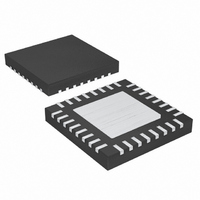
MAX1533AETJ+ Maxim Integrated Products, MAX1533AETJ+ Datasheet - Page 23

MAX1533AETJ+
Manufacturer Part Number
MAX1533AETJ+
Description
IC POWER SUPPLY CONTROLER 32TQFN
Manufacturer
Maxim Integrated Products
Datasheet
1.MAX1533AETJT.pdf
(38 pages)
Specifications of MAX1533AETJ+
Applications
Power Supply Controller
Voltage - Input
4.5 ~ 26 V
Current - Supply
15µA
Operating Temperature
-40°C ~ 85°C
Mounting Type
Surface Mount
Package / Case
32-TQFN Exposed Pad
Lead Free Status / RoHS Status
Lead free / RoHS Compliant
Voltage - Supply
-
Lead Free Status / Rohs Status
Lead free / RoHS Compliant
DC output accuracy specifications in the Electrical
Characteristics table refer to the error-comparator’s
threshold. When the inductor continuously conducts,
the MAX1533A/MAX1537A regulate the peak of the out-
put ripple, so the actual DC output voltage is lower than
the slope-compensated trip level by 50% of the output
ripple voltage. For PWM operation (continuous conduc-
tion), the output voltage is accurately defined by the fol-
lowing equation:
where V
equals 1%, and V
(V
Output Capacitor Selection section).
In discontinuous conduction (I
MAX1533A/MAX1537A regulate the valley of the output
ripple, so the output voltage has a DC regulation level
higher than the error-comparator threshold. For PFM
operation (discontinuous conduction), the output volt-
age is approximately defined by the following equation:
Figure 4. Pulse-Skipping/Discontinuous Crossover Point
V
OUT PWM
RIPPLE
High-Efficiency, 5x Output, Main Power-Supply
(
0
NOM
= ESR x ΔI
)
ON-TIME
=
is the nominal output voltage, A
V
NOM
______________________________________________________________________________________
RIPPLE
t
ON(SKIP)
⎛
⎜
⎝
INDUCTOR
1
≥
-
V
is the output ripple voltage
IN
A
I
IDLE
Controllers for Notebook Computers
- V
SLOPE NOM
OUT
L
OUT
TIME
V
IN
as described in the
V
Output Voltage
< I
LOAD(SKIP)
⎞
⎟
⎠
I
LOAD(SKIP)
-
⎛
⎜
⎝
V
RIPPLE
2
SLOPE
), the
⎞
⎟
⎠
where V
maximum switching frequency set by the internal oscil-
lator, f
the idle-mode inductor current when pulse skipping.
Connect FB3 and FB5 to GND to enable the fixed
SMPS output voltages (3.3V and 5V, respectively), set
by a preset, internal resistive voltage-divider connected
between CSL_ and analog ground. Connect a resistive
voltage-divider at FB_ between CSL_ and GND to
adjust the respective output voltage between 1V and
5.5V (Figure 5). Choose R2 (resistance from FB to
GND) to be about 10kΩ and solve for R1 (resistance
from OUT to FB) using the equation:
where V
Figure 5. Dual-Mode Feedback Decoder
AMPLIFIER
TO ERROR
V
OUT PFM
SW
(2.0V)
CSL
REF
FB_
NOM
FB
is the actual switching frequency, and I
(
= 1V nominal.
is the nominal output voltage, f
)
R
R
=
1
V
12R
NOM
=
Adjustable/Fixed Output Voltages
R
2
+
⎛
⎜
⎝
2
1
V
V
⎛
⎜
⎝
OUT
FB
f
f
OSC
FIXED OUTPUT
SW
(Dual-Mode Feedback)
ADJUSTABLE
_
FB = GND
_
OUTPUT
⎞
⎟
⎠
−
I
IDLE
1
⎞
⎟
⎠
×
OSC
ESR
IDLE
is the
23
is


