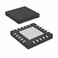
IR3082AMTRPBF International Rectifier, IR3082AMTRPBF Datasheet - Page 21

IR3082AMTRPBF
Manufacturer Part Number
IR3082AMTRPBF
Description
IC XPHASE CONTROL 9.6V 20-MLPQ
Manufacturer
International Rectifier
Series
XPhase™r
Datasheet
1.IR3082AMTRPBF.pdf
(33 pages)
Specifications of IR3082AMTRPBF
Applications
Processor
Current - Supply
12mA
Voltage - Supply
8.05 V ~ 16 V
Operating Temperature
0°C ~ 100°C
Mounting Type
Surface Mount
Package / Case
20-MLPQ
Ic Function
Control IC
Supply Voltage Range
8.05V To 16V
Operating Temperature Range
0°C To +100°C
Digital Ic Case Style
MLPQ
No. Of Pins
20
Filter Terminals
SMD
Supply Voltage Min
9.6V
Rohs Compliant
Yes
Controller Type
PWM
Frequency
1MHz
Package
20-Lead MLPQ
Circuit
X-Phase Control IC
Switch Freq (khz)
150kHz to 1.0MHz
Pbf
PbF Option Available
Lead Free Status / RoHS Status
Lead free / RoHS Compliant
Other names
IR3082AMTRPBFTR
No Load Output Voltage Setting Resistor R
A resistor between FB pin and the converter output is used to create output voltage offset V
difference between V
converter voltage by Ro times Io, where Ro is the required output impedance of the converter.
R
the total input offset voltage of current sense amplifiers. R
respectively.
IR3086A EXTERNAL COMPONENTS
PWM Ramp Resistor R
PWM ramp is generated by connecting the resistor R
as the capacitor C
the capacitor C
(17). To achieve feed-forward voltage mode control, the resistor R
converter.
Inductor Current Sensing Capacitor C
The DC resistance of the inductor is utilized to sense the inductor current. Usually the resistor R
C
across the capacitor C
component of the capacitor voltage is different from that of the real inductor current. The time constant mismatch
does not affect the average current sharing among the multiple phases, but affect the current signal ISHARE as well
as the output voltage during the load current transient if adaptive voltage positioning is adopted.
Measure the inductance L and the inductor DC resistance R
follows.
The bias current flowing out of the non-inverting input of the current sense amplifier creates a voltage drop across
R
converter current signal ISHARE as well as the accuracy of the converter output voltage if adaptive voltage
positioning is adopted. To reduce the offset voltage, a resistor R
input and the converter output
input and the bias current from the inverting input.
FB
CS+
CS+,
is not only determined by I
in parallel with the inductor are chosen to match the time constant of the inductor, and therefore the voltage
which is equivalent to an input offset voltage of the current sense amplifier. The offset affects the accuracy of
Page 21 of 33
PWMRMP
R
R
R
R
R
FB
DRP
PWMRMP
CS
CS
PWMRMP
DAC
R
CS+
L
C
I
I
R
L
PWMRMP
in the range of 100pF and 470pF, and then calculate the resistor R
CSIN
CSIN
_
CS
FB
R
voltage and output voltage at no load condition. Adaptive voltage positioning lowers the
MAX
V
L
˜
between PWMRMP and LGND. Choose the desired PWM ramp magnitude V
IN
represents the inductor current. If the two time constants are not the same, the AC
R
˜
˜
L
.
˜
R
V
_
The resistor R
FB
n
f
CS
O
MAX
SW
˜
_
and Capacitor C
, the current flowing out of the FB pin as shown in Figure 14, but also affected by
R
I
NLOFST
FB
O
˜
˜
C
G
˜
PWMRMP
R
CS
L
_
CS+
_
V
MIN
MAX
CS
˜
_
and Resistors R
[ln(
CS-
TOFST
FB
V
and Adaptive Voltage Positioning Resistor R
is determined by the ratio of the bias current from the non-inverting
IN
˜
PWMRMP
n
˜
V
R
PWMRMP
V
DAC
O
O
)
L
ln(
. Pre-select the capacitor C
CS+
between a voltage source and PWMRMP pin as well
V
CS-
FB
IN
and R
should be added between the amplifier inverting
and R
V
RAMP
DAC
CS-
should be connected to the input of the
V
DRP
PWMRMP
are determined by (15) and (16)
)]
CS+
(
(17)
(18)
(19)
(15)
16)
PWMRMP
O_NLOFST,
and calculate R
05/02/2006
DRP
IR3082A
CS+
from Equation
and capacitor
which is the
RAMP
CS+
and
as


