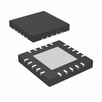
IR3082AMTRPBF International Rectifier, IR3082AMTRPBF Datasheet - Page 11

IR3082AMTRPBF
Manufacturer Part Number
IR3082AMTRPBF
Description
IC XPHASE CONTROL 9.6V 20-MLPQ
Manufacturer
International Rectifier
Series
XPhase™r
Datasheet
1.IR3082AMTRPBF.pdf
(33 pages)
Specifications of IR3082AMTRPBF
Applications
Processor
Current - Supply
12mA
Voltage - Supply
8.05 V ~ 16 V
Operating Temperature
0°C ~ 100°C
Mounting Type
Surface Mount
Package / Case
20-MLPQ
Ic Function
Control IC
Supply Voltage Range
8.05V To 16V
Operating Temperature Range
0°C To +100°C
Digital Ic Case Style
MLPQ
No. Of Pins
20
Filter Terminals
SMD
Supply Voltage Min
9.6V
Rohs Compliant
Yes
Controller Type
PWM
Frequency
1MHz
Package
20-Lead MLPQ
Circuit
X-Phase Control IC
Switch Freq (khz)
150kHz to 1.0MHz
Pbf
PbF Option Available
Lead Free Status / RoHS Status
Lead free / RoHS Compliant
Other names
IR3082AMTRPBFTR
IR3082A THEORY OF OPERATION
Block Diagram
The Block diagram of the IR3082A is shown in figure 7 and discussed in the following sections.
VID Control
A 5-bit VID voltage compatible with AMD’s Opteron/Athlon64, as shown in Table 1, is available at the VDAC pin.
The VID pins require an external bias voltage and should not be floated. The VID input comparators, with 1.2V
reference, monitor the VID pins and control the 6 bit Digital-to-Analog Converter (DAC) whose output is sent to the
VDAC buffer amplifier. The output of the buffer amp is the VDAC pin. The VDAC voltage is trimmed to compensate
for the input offsets of the Error Amp to provide 1% system set-point accuracy and is pre-positioned 50mV higher
than Vout listed in Table1 for load positioning. The actual VDAC voltage does not determine the system accuracy
and has a wider tolerance.
The IR3082A can accept changes in the VID code while operating and vary the DAC voltage accordingly. The
sink/source capability of the VDAC buffer amp is programmed by the same external resistor that sets the oscillator
frequency. The slew rate of the voltage at the VDAC pin can be adjusted by an external capacitor between VDAC
pin and the VOSNS- pin. A resistor connected in series with this capacitor is required to compensate the VDAC
buffer amplifier. Digital VID transitions result in a smooth analog transition of the VDAC voltage and converter
output voltage minimizing inrush currents in the input and output capacitors and overshoot of the output voltage.
Page 11 of 33
ENABLE
VOSNS-
RMPOUT
SS/DEL
ROSC
VCC
VID4
VID3
VID2
VID1
VID0
8.25V
7.70V
+
-
+
-
1.27V
1.21V
IHICCUP
IDISCHG
5uA
+
-
-
+
+
-
1.22V
ROSC
BUFFER
AMP
-
+
VCC
COMPARATOR
50%
DUTY
CYCLE
+
-
VID INPUT
COMPARATORS
(1 OF 5
SHOWN)
ENABLE
COMPARATOR
UVLO
VCHG
3.9V
RAMP GENERATOR
ICHG
55uA
+
-
ON
CURRENT
SOURCE
GENERATOR
65mV
110mV
OFF
0.22V
Figure 7 – IR3082A Block Diagram
DIGITAL TO
ANALOG
CONVERTER
+
-
OC
DISCHG
CURRENT
35uA
5.0V
1.0V
"FAST"
-
+
+
-
VDAC
DISCHARGE
COMPARATOR
DELAY
COMPARATOR
IROSC
VBIAS
SS/DEL
DISCHARGE
ON
+
-
1.3V
SOFTSTART
CLAMP
+
-
ISOURCE
ISINK
VDAC
BUFFER
AMP
450ns
BLANKING
IOCSET
COMPARATOR
OC
+
-
IROSC
FAULT
LATCH
S
R
VBIAS
REGULATOR
DISABLE
IFB
IROSC
+
-
+
-
+
ERROR
AMP
+
-
05/02/2006
VDRP
AMP
IR3082A
+
-
6.3V
PWRGD
VDRP
IIN
OCSET
EAOUT
FB
LGND
VDAC
VBIAS


