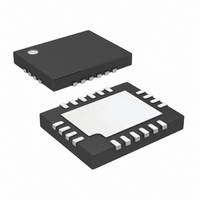
LT3751EUFD#PBF Linear Technology, LT3751EUFD#PBF Datasheet - Page 22

LT3751EUFD#PBF
Manufacturer Part Number
LT3751EUFD#PBF
Description
IC CAPACITOR CHRG 20-QFN
Manufacturer
Linear Technology
Datasheet
1.LT3751EUFDPBF.pdf
(34 pages)
Specifications of LT3751EUFD#PBF
Applications
Photoflash Capacitor Charger
Current - Supply
5.5mA
Voltage - Supply
4.75 V ~ 24 V
Operating Temperature
-40°C ~ 125°C
Mounting Type
Surface Mount
Package / Case
20-QFN
Primary Input Voltage
24V
No. Of Outputs
1
No. Of Pins
20
Operating Temperature Range
-40°C To +125°C
Msl
MSL 1 - Unlimited
Supply Voltage Range
4.75V To 24V
Termination Type
SMD
Rohs Compliant
Yes
Lead Free Status / RoHS Status
Lead free / RoHS Compliant
Available stocks
Company
Part Number
Manufacturer
Quantity
Price
APPLICATIONS INFORMATION
LT3751
Large Signal Stability
Large signal stability can be an issue when audible noise
is a concern. Figure 12 shows that the problem originates
from the one-shot clock and the output voltage ripple. The
load must be constrained such that the output voltage
ripple does not exceed the regulation range of the error
amplifi er within one clock period (approximately 6mV
referred to the FB pin).
The output capacitance should be increased if oscillations
occur or audible noise is present. Use Figure 13 to determine
the maximum load for a given output capacitance to
maintain low audible noise operation. A small capacitor
can also be added from the FB pin to ground to lower the
ripple injected into FB pin.
22
ONE-SHOT
26kHz
V
CLK
I
OUT
PRI
Figure 12. Voltage Ripple Stability Constraint
30
25
20
15
10
5
0
Figure 13. C
0
V
V
V
50
OUT
OUT
OUT
OUTPUT POWER (W)
OUT(MIN)
= 150V
= 300V
= 600V
100
DROOP
LOAD
vs Output Power
150
3751 F14
200
3751 F13
Small Signal Stability
The LT3751’s error amplifi er is internally compensated to
increase its operating range but requires the converter’s
output node to be the dominant pole. Small signal stability
constraints become more prevalent during heavy loading
conditions where the dominant output pole moves to
higher frequency and closer to the internal feedback
poles and zeros. The feedback loop requires the output
pole frequency to remain below 200Hz to guarantee small
signal stability. This allows smaller R
large signal constraint. Thus, small signal issues should
not arise if the large signal constraint is met.
Board Layout
The high voltage operation of the LT3751 demands careful
attention to the board layout, observing the following
points:
1. Minimize the area of the high voltage end of the
2. Provide suffi cient spacing for all high voltage nodes
3. Keep the electrical path formed by C
4. Reduce the total node capacitance on the RV
5. Thermal vias should be added underneath the
6. Isolated applications require galvanic separation of the
secondary winding.
(NMOS drain, V
transformer) in order to meet the breakdown voltage
requirements.
of T1, and the drain of the NMOS as short as possible.
Increasing the length of this path effectively increases
the leakage inductance of T1, potentially resulting in an
overvoltage condition on the drain of the NMOS.
Exposed Pad, Pin 21, to enhance the LT3751’s thermal
performance. These vias should go directly to a large
area of ground plane.
output-side ground and primary-side ground. Adequate
spacing between both ground planes is needed to meet
voltage safety requirements.
R
underneath the R
Parasitic capacitance can cause unwanted behavior
on these pins.
DCM
pins by removing any ground or power planes
OUT
DCM
and secondary winding of the
and R
VOUT
LOAD
VTRANS
pads and traces.
values than the
, the primary
OUT
3751fb
and


