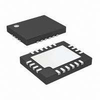
LT3751EUFD#PBF Linear Technology, LT3751EUFD#PBF Datasheet - Page 12

LT3751EUFD#PBF
Manufacturer Part Number
LT3751EUFD#PBF
Description
IC CAPACITOR CHRG 20-QFN
Manufacturer
Linear Technology
Datasheet
1.LT3751EUFDPBF.pdf
(34 pages)
Specifications of LT3751EUFD#PBF
Applications
Photoflash Capacitor Charger
Current - Supply
5.5mA
Voltage - Supply
4.75 V ~ 24 V
Operating Temperature
-40°C ~ 125°C
Mounting Type
Surface Mount
Package / Case
20-QFN
Primary Input Voltage
24V
No. Of Outputs
1
No. Of Pins
20
Operating Temperature Range
-40°C To +125°C
Msl
MSL 1 - Unlimited
Supply Voltage Range
4.75V To 24V
Termination Type
SMD
Rohs Compliant
Yes
Lead Free Status / RoHS Status
Lead free / RoHS Compliant
Available stocks
Company
Part Number
Manufacturer
Quantity
Price
OPERATION
LT3751
At very low output voltages, the boundary-mode switching
cycle period increases signifi cantly such that the energy
stored in the transformer core is not depleted before the
next clock cycle. In this situation, the clock may initiate
another switching cycle before the secondary winding
current reaches zero and cause the LT3751 to enter con-
tinuous-mode conduction. Normally, this is not a problem;
however, if the secondary energy transfer time is much
longer than the CLK period, signifi cant primary current
overshoot can occur. This is due to the non-zero starting
point of the primary current when the switch turns on and
the fi nite speed of the current comparator.
The LT3751 startup circuitry adds an auxiliary current
comparator with a trip level 50% higher than the nominal
trip level. Every time the auxiliary current comparator
trips, the required clock count between switching cycles is
incremented by one. This allows more time for secondary
energy transfer.
Counter 1 in Figure 3 is set to its maximum count when
the fi rst DCM comparator one-shot is generated. If no
DCM one-shot is initiated in normal boundary-mode
operation during a maximum count of approximately
500μs, the LT3751 re-enters start-up mode and the count
is returned to zero.
Note that Counter 1 is initialized to zero at start-up. Thus,
the output of the startup circuitry will go high after one clock
cycle. Counter 2 is reset when the gate driver goes high.
This repeats until either the auxiliary current comparator
increments the required clock count or until V
enough to sustain normal operation described in steps 2
through 4 in the previous section.
Entering Normal Boundary Mode
The LT3751 has two DCM comparator thresholds that are
dependent on what mode the part is in, either start-up
mode or normal boundary-mode, and the state of the mode
latch. For boundary-mode switching, the LT3751 requires
the DCM sense voltage (V
ΔDCM comparator threshold, ΔV
where I
signal is negative edge triggered by the switch node,
12
ΔV
DRAIN
OFFSET
= (40μA + I
is mode dependent. The DCM one-shot
OFFSET
DRAIN
) • R
) to exceed V
DRAIN
DCM
– 40μA • RV
:
TRANS
DRAIN
is high
by the
TRANS
V
winding has depleted. For this to happen, V
exceed V
erwise, the DCM comparator will not generate a one-shot
to initiate the next switching cycle. The part would remain
stuck in this state indefi nitely; however, the LT3751 uses
the start-up protection circuitry to jumpstart switching if
the DCM comparator does not generate a one-shot after
a maximum time-out of 500μs.
Figure 4 shows a typical V
a test circuit voltage clamp applied to the output. V
is the start-up threshold and is set internally by forcing
I
the mode latch is set to boundary-mode. The mode latch
then sets the clock count to maximum (500μs) and lowers
the DCM comparator threshold to V
This provides needed hysteresis between start-up mode
and boundary-mode operation.
LOW NOISE REGULATION
Low noise voltage regulation can be achieved by adding
a resistive divider from the output node to the LT3751 FB
pin. At start-up (FB pin below 1.16V), the LT3751 enters
the charge mode to rapidly charge the output capacitor.
Once the FB pin is within the threshold range of 1.16V
to 1.34V, the part enters into low noise regulation. The
switching methodology in regulation mimics that used
in the capacitor charging mode, but with the addition of
peak current and duty cycle control techniques. Figure 5
shows the steady state operation for both regulation
techniques. Figure 6 shows how both techniques are
combined to provide stable, low noise operation over a
wide load and supply range.
During heavy load conditions, the LT3751 sets the peak
primary current to its maximum value, 106mV/R
sets the maximum duty cycle to approximately 95%. This
allows for maximum power delivery. At very light loads,
the opposite occurs, and the LT3751 reduces the peak
primary current to approximately one tenth its maximum
value while modulating the duty cycle below 10%. The
LT3751 controls moderate loads with a combination of
peak current mode control and duty cycle control.
OFFSET
DRAIN
, and indicates that the energy in the secondary
to 40μA. Once the fi rst DCM one-shot is initiated,
TRANS
+ ΔV
DRAIN
prior to its negative edge; oth-
DRAIN
node waveform with
TH2
(I
OFFSET
DRAIN
SENSE
= 20μA).
must
3751fb
and
TH1


