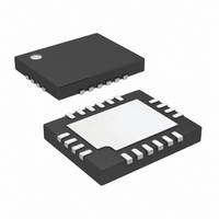
LT3751EUFD#PBF Linear Technology, LT3751EUFD#PBF Datasheet - Page 21

LT3751EUFD#PBF
Manufacturer Part Number
LT3751EUFD#PBF
Description
IC CAPACITOR CHRG 20-QFN
Manufacturer
Linear Technology
Datasheet
1.LT3751EUFDPBF.pdf
(34 pages)
Specifications of LT3751EUFD#PBF
Applications
Photoflash Capacitor Charger
Current - Supply
5.5mA
Voltage - Supply
4.75 V ~ 24 V
Operating Temperature
-40°C ~ 125°C
Mounting Type
Surface Mount
Package / Case
20-QFN
Primary Input Voltage
24V
No. Of Outputs
1
No. Of Pins
20
Operating Temperature Range
-40°C To +125°C
Msl
MSL 1 - Unlimited
Supply Voltage Range
4.75V To 24V
Termination Type
SMD
Rohs Compliant
Yes
Lead Free Status / RoHS Status
Lead free / RoHS Compliant
Available stocks
Company
Part Number
Manufacturer
Quantity
Price
APPLICATIONS INFORMATION
Two problems can arise from large V
magnitude of the spike may require an NMOS with an
unnecessarily high V
R
below ground—causing false tripping of the DCM
comparator or damage to the NMOS switch (see Figure
11). Both issues can be remedied using a snubber. If
leakage inductance causes issues, it is recommended to
use a RC snubber in parallel with the primary winding, as
shown in Figure 10. Size C
desired leakage spike voltage, known leakage inductance,
and an RC time constant less than 1μs. Otherwise, the
leakage voltage spike can cause false tripping of the V
comparator and stop charging prematurely.
Figure 11 shows the effect of the RC snubber resulting in
a lower voltage spike and faster settling time.
SNUBBER)
SNUBBER)
(WITHOUT
DS(ON)
V
V
(WITH
DRAIN
DRAIN
I
PRI
0V
0V
. Secondly, the V
Figure 11. Effects of RC Snubber
Figure 10. RC Snubber Circuit
NMOS DIODE
CONDUCTS
R
SNUB
C
SNUB
(BR)DSS
L
LEAK
L
PRI
DRAIN
SNUB
•
which equates to a larger
•
node will ring—possibly
and R
C
VDRAIN
3751 F11
SNUB
D,LEAK
based on the
. First, the
3751 F12
OUT
LOW NOISE REGULATION
The LT3751 has the option to provide a low noise regulated
output voltage when using a resistive voltage divider
from the output node to the FB pin. Refer to the Selecting
Component Parameters section to design the transformer,
NMOS power switch, output diode, and sense resistor.
Use the following equations to select the feedback resistor
values based on the power dissipation and desired output
voltage:
R
require several smaller values placed in series. This will
reduce the risk of arcing and damage to the feedback
resistors. Consult the manufacturer’s rated voltage
specifi cation for safe operation of the feedback resistors.
The LT3751 has a minimum periodic refresh frequency
limit of 23kHz. This drastically reduces switching frequency
components in the audio spectrum. The LT3751 can
operate with no-load, but the regulation scheme switches
to no-load operation and audible noise and output voltage
ripple increase. This can be avoided by operating with a
minimum load current.
Minimum Load Current
Periodic refresh circuitry requires an average minimum
load current to avoid entering no-load operation. Usually,
the feedback resistors should be adequate to provide this
minimum load current.
I
The LT3751 will enter no-load operation if the minimum
load current is not met. No-load operation will prevent the
application from entering a runaway condition; however,
the output voltage will increase 10% over the nominal
regulated voltage.
R
R
PK
FBH
FBH
FBL
I
is the peak primary current at maximum power delivery.
LOAD(MIN)
, depending on output voltage and type used, may
=
=
⎛
⎝ ⎜
(
V
V
OUT
OUT
1.22
P
≥
− 1.22
− 1.22
D
L
PRI
100 • V
)
•I
⎞
⎠ ⎟
2
• R
2
; Top Feedback Resistor
PK
FBH
• 23kHz
OUT
; Bottom Feedback Resistor
LT3751
21
3751fb


