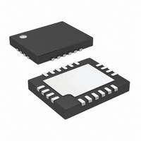
LT3751EUFD#PBF Linear Technology, LT3751EUFD#PBF Datasheet - Page 15

LT3751EUFD#PBF
Manufacturer Part Number
LT3751EUFD#PBF
Description
IC CAPACITOR CHRG 20-QFN
Manufacturer
Linear Technology
Datasheet
1.LT3751EUFDPBF.pdf
(34 pages)
Specifications of LT3751EUFD#PBF
Applications
Photoflash Capacitor Charger
Current - Supply
5.5mA
Voltage - Supply
4.75 V ~ 24 V
Operating Temperature
-40°C ~ 125°C
Mounting Type
Surface Mount
Package / Case
20-QFN
Primary Input Voltage
24V
No. Of Outputs
1
No. Of Pins
20
Operating Temperature Range
-40°C To +125°C
Msl
MSL 1 - Unlimited
Supply Voltage Range
4.75V To 24V
Termination Type
SMD
Rohs Compliant
Yes
Lead Free Status / RoHS Status
Lead free / RoHS Compliant
Available stocks
Company
Part Number
Manufacturer
Quantity
Price
APPLICATIONS INFORMATION
The LT3751 charger controller can be optimized for either
capacitor charging only or low noise regulation applica-
tions. Several equations are provided to aid in the design
process.
Safety Warning
Large capacitors charged to high voltage can deliver a lethal
amount of energy if handled improperly. It is particularly
important to observe appropriate safety measures when
designing the LT3751 into applications. First, create a dis-
charge circuit that allows the designer to safely discharge
the output capacitor. Second, adequately space high voltage
nodes from adjacent traces to satisfy printed circuit board
voltage breakdown requirements.
Selecting Operating Mode
Tie the FB pin to GND to operate the LT3751 as a capacitor
charger. In this mode, the LT3751 charges the output at
peak primary current in boundary mode operation. This
constitutes maximum power delivery and yields the fast-
est charge times. Power delivery is halted once the output
reaches the desired output voltage set by the RV
RBG pins.
Tie a resistor divider from the FB pin to V
to operate the LT3751 as a low noise voltage regulator
(refer to Low Noise regulation section for proper design
procedures). The LT3751 operates as a voltage regulator
using both peak current and duty cycle modulation to vary
output current during different loading conditions.
Selecting Component Parameters
Most designs start with the initial selection of V
V
charger) or P
are then used to select the transformer ratio, N, the peak
primary current, I
Figure 7 can be used as a rough guide for maximum power
output for a given V
OUT
, C
OUT
, and either charge time, t
OUT,MAX
PK
TRANS
, and the primary inductance, L
(regulator). These design inputs
and I
PK
.
CHARGE
OUT
, (capacitor
and GND
OUT
TRANS
and
PRI
,
.
Selecting Transformer Turns Ratio
The transformer ratio, N, should be selected based on the
input and output voltages. Smaller N values equate to faster
charge times and larger available output power. Note that
drastically reducing N below the V
increase the fl yback voltage on the drain of the NMOS and
increase the current through the output diode. The ratio,
N, should not be drastically increased either, due to the
increased capacitance, N
A good choice is to select N equal to V
Choosing Capacitor Charger I
When operating the LT3751 as capacitor charger, choose
I
and the initial design inputs.
The converter effi ciency varies over the output voltage
range. The I
ciency over the entire charging period. Several factors can
cause the charge time to increase. Effi ciency is the most
dominant factor and is mainly affected by the transformer
winding resistance, core losses, leakage inductance, and
transistor R
above 70%.
PK
I
N ≤
based on the required capacitor charge time, t
PK
=
V
V
TRANS
(
OUT
Efficiency • V
2 • N • V
100
90
80
70
60
50
40
30
20
10
DS
0
PK
1
Figure 7. Maximum Power Output
. Most applications have overall effi ciencies
equation is based on the average effi -
TRANS
PEAK PRIMARY CURRENT (A)
TRANS
+ V
2
• C
OUT
10
SEC
• t
(
PK
)
, refl ected to the primary.
CHARGE
• C
P = 20 WATTS
P = 50 WATTS
P = 100 WATTS
OUT
OUT
OUT
/V
• V
− t
3751 F07
TRANS
100
OUT
/V
LT3751
d
)
TRANS
ratio will
CHARGE
15
.
3751fb
,


