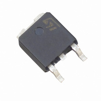
VND10N06 STMicroelectronics, VND10N06 Datasheet - Page 7

VND10N06
Manufacturer Part Number
VND10N06
Description
MOSFET N-CH 60V 10A DPAK
Manufacturer
STMicroelectronics
Series
OMNIFET™r
Type
Low Sider
Datasheet
1.VND10N06-1.pdf
(25 pages)
Specifications of VND10N06
Input Type
Non-Inverting
Number Of Outputs
1
On-state Resistance
150 mOhm
Current - Peak Output
10A
Mounting Type
Surface Mount
Package / Case
DPak, TO-252 (2 leads+tab), SC-63
Lead Free Status / RoHS Status
Contains lead / RoHS non-compliant
Voltage - Supply
-
Operating Temperature
-
Current - Output / Channel
-
Other names
497-2767-5
Available stocks
Company
Part Number
Manufacturer
Quantity
Price
Company:
Part Number:
VND10N06
Manufacturer:
ST
Quantity:
13 583
Company:
Part Number:
VND10N06-1
Manufacturer:
ST
Quantity:
12 500
Company:
Part Number:
VND10N06-1-E
Manufacturer:
IXYS
Quantity:
6 000
Company:
Part Number:
VND10N0613TR
Manufacturer:
ST
Quantity:
20 000
Company:
Part Number:
VND10N06TR-E
Manufacturer:
ST
Quantity:
20 000
Part Number:
VND10N06TR-E
Manufacturer:
ST
Quantity:
20 000
VND10N06 / VND10N06-1
2.3
Electrical characteristics
T
Table 4.
Table 5.
1. Parameters guaranteed by design / characterization.
Table 6.
1. Pulsed: pulse duration = 300µs, duty cycle 1.5%.
Symbol
Symbol
Symbol
case
V
(di/dt)
R
V
CLAMP
t
t
t
t
I
DS(on)
I
d(on)
d(off)
d(on)
d(off)
V
V
DSS
INCL
ISS
Q
t
t
t
t
IH
IL
r
r
f
f
i
= 25 °C unless otherwise stated.
on
Drain-Source clamp
voltage
Input low level voltage I
Input high Level
voltage
Supply current from
input pin
Input-Source reverse
clamp voltage
Zero input voltage
drain current
(V
Turn-on delay time
Rise time
Turn-off delay time
Fall time
Turn-on delay time
Rise time
Turn-off delay time
Fall time
Turn-on current slope
Total input charge
Static Drain-Source
on resistance
IN
Off
Switching
On
= 0V)
Parameter
Parameter
Parameter
(1)
(1)
V
R
V
V
I
I
V
V
V
D
IN
IN
V
V
(see
V
V
(see
V
V
V
IN
DS
DS
DS
DS
IN
L
DD
gen
DD
gen
DD
in
DD
= 100 µA; V
= -1mA
= 1mA
= 27Ω; V
= 0V; I
= 7V; I
= 7V; R
= 0V; V
= 50V; V
< 35V; V
= 0.5 V
= 16V; I
= 16V; I
= 16V; I
= 12V; I
= 7V; R
Figure
= 7V; R
Figure
Test conditions
Test conditions
Test conditions
D
D
gen
DD
IN
= 200mA
= 1 A; T
2)
2)
IN
IN
D
D
D
D
gen
gen
= 5V
DS
= 16 V
= 1A
= 1A
= 1A
= 1A; V
= 10Ω
= V
= V
= 10Ω
= 1000Ω
= 16 V
IL
IL
j
;
< 125 °C
IN
= 7V
Min.
Min.
Min.
3.2
Electrical specifications
50
-1
8
1100
Typ.
Typ.
Typ.
0.15
150
550
200
100
1.2
1.6
1.2
1.5
60
13
1
Max.
1600
Max.
Max.
-0.3
300
250
100
900
400
200
1.5
0.3
1.8
1.5
2.3
1.8
70
11
A/µs
Unit
Unit
Unit
nC
µA
µA
µA
ns
ns
ns
ns
µs
µs
µs
µs
V
V
V
V
V
Ω
7/25


