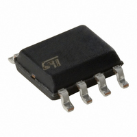
VN750S-E STMicroelectronics, VN750S-E Datasheet - Page 8

VN750S-E
Manufacturer Part Number
VN750S-E
Description
IC DRIVER HIGH SIDE 8-SOIC
Manufacturer
STMicroelectronics
Type
High Sider
Specifications of VN750S-E
Input Type
Non-Inverting
Number Of Outputs
1
On-state Resistance
60 mOhm
Current - Peak Output
6A
Voltage - Supply
5.5 V ~ 36 V
Operating Temperature
-40°C ~ 150°C
Mounting Type
Surface Mount
Package / Case
8-SOIC (3.9mm Width)
Supply Voltage (min)
5.5 V
Supply Current
3.5 mA
Maximum Power Dissipation
4200 mW
Maximum Operating Temperature
+ 150 C
Mounting Style
SMD/SMT
Maximum Turn-off Delay Time
30000 ns
Maximum Turn-on Delay Time
40000 ns
Minimum Operating Temperature
- 40 C
Number Of Drivers
1
Device Type
High Side
Module Configuration
High Side
Peak Output Current
6A
Output Resistance
0.06ohm
Input Delay
40µs
Output Delay
30µs
Supply Voltage Range
5.5V To 36V
Driver Case Style
SOIC
Rohs Compliant
Yes
Lead Free Status / RoHS Status
Lead free / RoHS Compliant
Current - Output / Channel
-
Lead Free Status / Rohs Status
Lead free / RoHS Compliant
Available stocks
Company
Part Number
Manufacturer
Quantity
Price
Electrical specifications
Table 5.
8/37
Switching (V
dV
dV
Input pin
V
Status pin
CC
Symbol
OUT
OUT
I
I
I
I
V
I
C
t
t
L(off1)
L(off2)
L(off3)
L(off4)
V
LSTAT
R
V
V
d(on)
d(off)
V
V
output diode
STAT
I
V
STAT
I
I
hyst
OV
ON
IH
ICL
IL
S
IH
IL
F
/dt
/dt
(on)
(off)
Electrical characteristics (continued)
CC
Overvoltage shutdown
On-state resistance
Supply current
Off-state output current
Off-state output current
Off-state output current
Off-state output current
Turn-on delay time
Turn-off delay time
Turn-on voltage slope
Turn-off voltage slope
Input low level
Low level input current
Input high level
High level input current
Input hysteresis voltage
Input clamp voltage
Forward on voltage
Status low output voltage I
Status leakage current
Status pin input
capacitance
=13 V)
Parameter
I
I
Off-state; V
Off-state; V
T
On-state; V
I
V
V
V
V
R
V
R
V
R
V
R
V
V
V
I
I
-I
Normal operation; V
Normal operation; V
OUT
OUT
OUT
IN
IN
STAT
j
OUT
OUT
OUT
OUT
OUT
IN
IN
IN
IN
L
L
L
L
IN
IN
=25
=1 mA
=-1 mA
=6.5 Ω from V
=6.5 Ω from V
=6.5 Ω from V
=6.5 Ω from V
=V
=0V; V
=V
=V
=1.25 V
=3.25 V
=2 A; T
=2 A; V
=0 A
=1.6 mA
=1.3 A; T
=1.3 V
=11.7 V
=10.4 V
=1.3 V
°C
OUT
OUT
OUT
Doc ID 10891 Rev 4
=0 V
=0 V; Vcc=13 V; T
=0 V; Vcc=13 V; T
OUT
CC
CC
CC
j
Test conditions
CC
=25 °C; V
=3.5 V
=13 V; V
=13 V; V
=13 V; V
j
>8 V
=150 °C
IN
IN
OUT
OUT
rising edge to
falling edge to
STAT
STAT
=1.3 V to
=11.7 V to
CC
IN
IN
IN
=5 V
=5 V
=V
=V
=5 V;
> 8 V
OUT
OUT
j
j
=125 °C
=25 °C
=0 V
=0 V;
Min.
3.25
-75
0.5
36
0
1
6
See
See
Figure 21.
Figure 22.
Typ.
-0.7
6.8
10
10
40
30
2
Max.
1.25
120
100
3.5
0.6
0.5
60
25
20
50
10
10
0
5
3
8
VN750-E
Unit
V/µs
V/µs
mΩ
mΩ
mA
µA
µA
µA
µA
µA
µA
µA
µA
µA
pF
µs
µs
V
V
V
V
V
V
V
V


