VNP10N06-E STMicroelectronics, VNP10N06-E Datasheet - Page 2
VNP10N06-E
Manufacturer Part Number
VNP10N06-E
Description
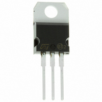
MOSFET OMNIFET 60V 10A TO-220
Manufacturer
STMicroelectronics
Series
OMNIFET™r
Type
Low Sider
Datasheet
1.VNP10N06.pdf
(11 pages)
Specifications of VNP10N06-E
Input Type
Non-Inverting
Number Of Outputs
1
On-state Resistance
150 mOhm
Current - Peak Output
10A
Mounting Type
Through Hole
Package / Case
TO-220-3 (Straight Leads)
Transistor Polarity
N-Channel
Resistance Drain-source Rds (on)
0.15 Ohms
Drain-source Breakdown Voltage
60 V
Gate-source Breakdown Voltage
+/- 20 V
Continuous Drain Current
10 A
Power Dissipation
42000 mW
Mounting Style
Through Hole
Lead Free Status / RoHS Status
Lead free / RoHS Compliant
Voltage - Supply
-
Operating Temperature
-
Current - Output / Channel
-
Lead Free Status / Rohs Status
Lead free / RoHS Compliant
Available stocks
Company
Part Number
Manufacturer
Quantity
Price
Company:

Part Number:
VNP10N06-E
Manufacturer:
NXP
Quantity:
9 000
Part Number:
VNP10N06-E
Manufacturer:
ST
Quantity:
20 000


VNP10N06
ABSOLUTE MAXIMUM RATING
THERMAL DATA
ELECTRICAL CHARACTERISTICS (T
OFF
ON ( )
DYNAMIC
2/11
Symbol
Symbol
Symbol
Symbol
R
R
V
R
V
V
V
T
thj-case
P
CLAMP
C
thj-amb
I
V
DS(on)
I
T
V
I
V
I
I
T
DSS
esd
INCL
I SS
DS
stg
in
D
R
tot
oss
in
c
IH
j
IL
Drain-source Voltage (V
Input Voltage
Input Current
Drain Current
Reverse DC Output Current
Electrostatic Discharge (C= 100 pF, R=1.5 K )
Total Dissipation at T
Operating Junction Temperature
Case Operating Temperature
Storage Temperature
Thermal Resistance Junction-case
Thermal Resistance Junction-ambient
Drain-source Clamp
Voltage
Input Low Level
Voltage
Input High Level
Voltage
Input-Source Reverse
Clamp Voltage
Zero Input Voltage
Drain Current (V
Supply Current from
Input Pin
Static Drain-source On
Resistance
Output Capacitance
Parameter
Parameter
Parameter
in
Parameter
= 0)
c
= 25
in
I
I
R
V
I
I
V
V
V
V
V
= 0)
D
D
in
in
DS
DS
DS
DS
in
DS
L
o
= 200 mA
= 100 A
= -1 mA
= 1 mA
= 27
C
= 7 V
= 0.5 V
= 13 V
= 50 V
< 35 V
= 0 V
case
= 25
Test Conditions
Test Conditions
Test Conditions
V
V
I
D
f = 1 MHz
V
V
in
DD
V
o
V
in
in
= 1 A T
C unless otherwise specified)
DS
= 5 V
in
= 16 V
= V
= V
= 0
= 16 V
IL
IL
J
< 125
V
in
= 0
o
Max
C
Max
Internally Clamped
Internally Clamped
Internally Limited
Internally Limited
Internally Limited
-55 to 150
Min.
Min.
Min.
Value
3.2
4000
50
-1
8
-15
42
20
Typ.
Typ.
0.15
Typ.
62.5
150
350
60
3
Max.
Max.
Max.
-0.3
250
100
300
500
1.5
0.3
70
11
o
o
Unit
Unit
Unit
Unit
C/W
C/W
mA
pF
o
o
o
W
V
V
V
V
V
V
V
A
A
V
C
C
C
A
A
A
Related parts for VNP10N06-E
Image
Part Number
Description
Manufacturer
Datasheet
Request
R

Part Number:
Description:
STMicroelectronics [RIPPLE-CARRY BINARY COUNTER/DIVIDERS]
Manufacturer:
STMicroelectronics
Datasheet:
Part Number:
Description:
STMicroelectronics [LIQUID-CRYSTAL DISPLAY DRIVERS]
Manufacturer:
STMicroelectronics
Datasheet:

Part Number:
Description:
BOARD EVAL FOR MEMS SENSORS
Manufacturer:
STMicroelectronics
Datasheet:
Part Number:
Description:
NPN TRANSISTOR POWER MODULE
Manufacturer:
STMicroelectronics
Datasheet:
Part Number:
Description:
TURBOSWITCH ULTRA-FAST HIGH VOLTAGE DIODE
Manufacturer:
STMicroelectronics
Datasheet:
Part Number:
Description:
Manufacturer:
STMicroelectronics
Datasheet:
Part Number:
Description:
DIODE / SCR MODULE
Manufacturer:
STMicroelectronics
Datasheet:
Part Number:
Description:
DIODE / SCR MODULE
Manufacturer:
STMicroelectronics
Datasheet:
Part Number:
Description:
Search -----> STE16N100
Manufacturer:
STMicroelectronics
Datasheet:
Part Number:
Description:
Search ---> STE53NA50
Manufacturer:
STMicroelectronics
Datasheet:
Part Number:
Description:
NPN Transistor Power Module
Manufacturer:
STMicroelectronics
Datasheet:
Part Number:
Description:
DIODE / SCR MODULE
Manufacturer:
STMicroelectronics
Datasheet: