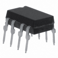
VO3150A Vishay, VO3150A Datasheet - Page 5

VO3150A
Manufacturer Part Number
VO3150A
Description
IC DRIVER IGBT/MOSFET 0.5A 8-DIP
Manufacturer
Vishay
Type
High Side/Low Side Driverr
Datasheet
1.VO3150A-X007T.pdf
(10 pages)
Specifications of VO3150A
Isolation Voltage
5300 Vrms
Input Type
Non-Inverting
Number Of Outputs
1
Current - Output / Channel
500mA
Current - Peak Output
500mA
Voltage - Supply
15 V ~ 32 V
Operating Temperature
-40°C ~ 110°C
Mounting Type
Through Hole
Package / Case
8-DIP (0.300", 7.62mm)
Fall Time
0.1 us
Logic Gate Type
IGBT
Rise Time
0.1 us
Configuration
1 Channel
Output Type
Integrated Photo IC
Maximum Propagation Delay Time
0.4 us
Maximum Forward Diode Voltage
1.6 V
Minimum Forward Diode Voltage
1 V
Maximum Reverse Diode Voltage
5 V
Maximum Forward Diode Current
25 mA
Maximum Continuous Output Current
0.5 A
Maximum Power Dissipation
295 mW
Maximum Operating Temperature
+ 110 C
Minimum Operating Temperature
- 40 C
No. Of Channels
1
Optocoupler Output Type
Gate Drive
Input Current
16mA
Output Voltage
500mV
Opto Case Style
DIP
No. Of Pins
8
Output Current
0.5A
Lead Free Status / RoHS Status
Lead free / RoHS Compliant
On-state Resistance
-
Lead Free Status / Rohs Status
Lead free / RoHS Compliant
Available stocks
Company
Part Number
Manufacturer
Quantity
Price
Company:
Part Number:
VO3150A
Manufacturer:
Vishay Semiconductors
Quantity:
1 899
Notes
(1)
(2)
(3)
Notes
(1)
(2)
(3)
Document Number: 81808
Rev. 1.1, 14-Jan-10
SWITCHING CHARACTERISTICS
PARAMETER
UVLO turn on delay
UVLO turn off delay
COMMON MODE TRANSIENT IMMUNITY
PARAMETER
Common mode transient immunity
at logic high output
Common mode transient immunity
at logic low output
This load condition approximates the gate load of a 1200 V/25 A IGBT.
Pulse width distortion (PWD) is defined as |t
The difference between t
Pins 1 and 4 need to be connected to LED common.
Common mode transient immunity in the high state is the maximum tolerable |dV
output will remain in the high state (i.e., V
Common mode transient immunity in a low state is the maximum tolerable |dV
output will remain in a low state (i.e., V
5 V
10 kHz
50 % duty
cycle
20980-1
20979_1
+
I
F
R
I = 7 mA to 16 mA
F
+
A
500 Ω
(1)(3)
(1)(2)
3
2
4
1
PHL
2
3
4
1
and t
V
CM
PLH
For technical questions, contact:
T
= 1500 V
A
between any two VO3150A parts under the same test condition.
O
= 25 °C, I
T
V
A
CM
< 1 V).
Fig. 7 - t
O
V
V
V
= 25 °C, V
TEST CONDITION
TEST CONDITION
O
O
CC
> 15 V).
PHL
= 1500 V, V
0.5 A Output Current IGBT and
> 5 V, I
> 5 V, I
= 32 V, V
Fig. 8 - CMR Test Circuit and Waveforms
- t
F
PLH
= 10 mA to 16 mA,
8
7
6
PLH
5
F
F
CM
, t
7
5
8
6
| for any given device.
= 10 mA
= 10 mA
PHL
CC
F
= 1500 V,
MOSFET Driver
= 0 V
, t
= 32 V
r
0.1 µF
and t
V
0.1 µF
O
47 Ω
f
3 nF
+
Test Circuit and Waveforms
V
optocoupleranswers@vishay.com
O
V
+
CC
SYMBOL
= 32 V
V
to 32 V
|CM
|CM
CC
SYMBOL
T
T
UVLO-OFF
= 15 V
UVLO-ON
H
L
|
|
CM
CM
V
Switch at B: I
Switch at A: I
V
0 V
O
O
/dt| of the common mode pulse, V
/dt| of the common mode pulse, V
I
F
MIN.
OUT
25
25
F
F
= 0 mA
= 10 mA
Dt
t
MIN.
PLH
Vishay Semiconductors
t
r
TYP.
35
35
TYP.
0.8
0.6
MAX.
t
PHL
CM
CM
MAX.
VO3150A
t
, to assure that the
, to assure that the
f
dV
dt
www.vishay.com
=
10 %
90 %
50 %
V
Dt
CM
kV/μs
kV/μs
UNIT
UNIT
μs
μs
V
V
OH
OL
5


