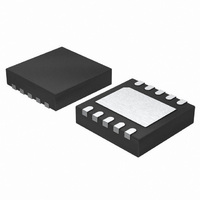
ISL6622BCRZ Intersil, ISL6622BCRZ Datasheet - Page 8

ISL6622BCRZ
Manufacturer Part Number
ISL6622BCRZ
Description
IC MOSFET DRVR SYNC BUCK 10-DFN
Manufacturer
Intersil
Datasheet
1.ISL6622BCBZ.pdf
(11 pages)
Specifications of ISL6622BCRZ
Configuration
High and Low Side, Synchronous
Input Type
PWM
Delay Time
20ns
Current - Peak
1.25A
Number Of Configurations
1
Number Of Outputs
2
High Side Voltage - Max (bootstrap)
36V
Voltage - Supply
6.8 V ~ 13.2 V
Operating Temperature
0°C ~ 70°C
Mounting Type
Surface Mount
Package / Case
10-DFN
Lead Free Status / RoHS Status
Lead free / RoHS Compliant
Available stocks
Company
Part Number
Manufacturer
Quantity
Price
Company:
Part Number:
ISL6622BCRZ
Manufacturer:
Intersil
Quantity:
25
Power Dissipation
Package power dissipation is mainly a function of the
switching frequency (F
layout resistance, and the selected MOSFET’s internal gate
resistance and total gate charge (Q
dissipation in the driver for a desired application is critical to
ensure safe operation. Exceeding the maximum allowable
power dissipation level may push the IC beyond the maximum
recommended operating junction temperature. The DFN
package is more suitable for high frequency applications. See
“Layout Considerations” on page 8 for thermal impedance
improvement suggestions. The total gate drive power losses
due to the gate charge of MOSFETs and the driver’s internal
circuitry and their corresponding average driver current can
be estimated with Equations 2 and 3, respectively:
where the gate charge (Q
particular gate to source voltage (V
corresponding MOSFET data sheet; I
quiescent current with no load at both drive outputs; N
and N
respectively; UVCC and LVCC are the drive voltages for
both upper and lower FETs, respectively. The I
product is the quiescent power of the driver without a load.
P
I
DR
Qg_TOT
FIGURE 4. BOOTSTRAP CAPACITANCE vs BOOT RIPPLE
P
P
=
Qg_Q1
Qg_Q2
Q2
1.6
1.4
1.2
1.0
0.8
0.6
0.4
0.2
0.0
⎛
⎜
⎝
Q
----------------------------------------------------- -
0.0
are number of upper and lower MOSFETs,
=
G1
20nC
P
=
•
=
0.1
Qg_Q1
VOLTAGE
UVCC N
V
Q
-------------------------------------- - F
Q
------------------------------------- - F
GS1
G1
G2
0.2
V
V
•
•
50nC
+
GS2
Q
GS1
•
UVCC
LVCC
P
GATE
SW
Qg_Q2
0.3
Q1
), the output drive impedance, the
G1
= 100nC
+
2
ΔV
2
0.4
•
Q
---------------------------------------------------- -
and Q
•
+
BOOT_CAP
8
G2
I
SW
Q
SW
0.5
•
•
G
LVCC N
•
VCC
V
GS1
G2
•
). Calculating the power
N
GS2
N
Q
0.6
Q2
) is defined at a
Q1
(V)
and V
is the driver’s total
•
0.7
Q2
GS2
⎞
⎟
⎠
Q*
0.8
•
VCC
F
) in the
SW
0.9
(EQ. 2)
(EQ. 3)
+
Q1
I
Q
1.0
ISL6622B
The total gate drive power losses are dissipated among the
resistive components along the transition path, as outlined in
Equation 4. The drive resistance dissipates a portion of the
total gate drive power losses, the rest will be dissipated by the
external gate resistors (R
resistors (R
the typical upper and lower gate drives turn-on current paths.
Application Information
Layout Considerations
During switching of the devices, the parasitic inductances of
the PCB and the power devices’ packaging (both upper and
lower MOSFETs) leads to ringing, possibly in excess of the
absolute maximum rating of the devices. Careful layout can
help minimize such unwanted stress. The following advice is
meant to lead to an optimized layout:
• Keep decoupling loops (LVCC-GND and BOOT-PHASE)
• Minimize trace inductance, especially low-impedance lines:
P
P
P
R
DR
DR_UP
DR_LOW
EXT1
FIGURE 6. TYPICAL LOWER-GATE DRIVE TURN-ON PATH
as short as possible.
all power traces (UGATE, PHASE, LGATE, GND, LVCC)
should be short and wide, as much as possible.
FIGURE 5. TYPICAL UPPER-GATE DRIVE TURN-ON PATH
UVCC
=
LVCC
P
=
DR_UP
=
R
=
GI1
⎛
⎜
⎝
G1
PHASE
--------------------------------------
R
⎛
⎜
⎝
R
HI1
--------------------------------------
R
R
+
BOOT
and R
LO2
HI2
R
HI2
R
+
R
-------------
R
N
LO1
HI1
+
P
GI1
HI1
R
Q1
DR_LOW
R
+
HI2
EXT1
R
GI2
EXT2
) of MOSFETs. Figures 5 and 6 show
G1
+
+
+
--------------------------------------- -
R
and R
I
LO1
--------------------------------------- -
R
R
Q
R
LO2
EXT2
L2
R
•
R
G
L1
VCC
+
LO1
R
G
G2
R
+
LO2
C
R
EXT1
R
) and the internal gate
GD
=
G2
C
R
EXT2
C
GD
G1
R
GS
C
G2
GS
⎞
⎟
⎠
•
⎞
⎟
⎠
S
+
P
---------------------
•
S
R
-------------
N
Qg_Q1
P
---------------------
GI2
Qg_Q2
Q2
2
D
2
D
March 19, 2009
Q2
C
Q1
DS
C
(EQ. 4)
DS


