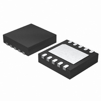
ISL6622BCRZ Intersil, ISL6622BCRZ Datasheet - Page 7

ISL6622BCRZ
Manufacturer Part Number
ISL6622BCRZ
Description
IC MOSFET DRVR SYNC BUCK 10-DFN
Manufacturer
Intersil
Datasheet
1.ISL6622BCBZ.pdf
(11 pages)
Specifications of ISL6622BCRZ
Configuration
High and Low Side, Synchronous
Input Type
PWM
Delay Time
20ns
Current - Peak
1.25A
Number Of Configurations
1
Number Of Outputs
2
High Side Voltage - Max (bootstrap)
36V
Voltage - Supply
6.8 V ~ 13.2 V
Operating Temperature
0°C ~ 70°C
Mounting Type
Surface Mount
Package / Case
10-DFN
Lead Free Status / RoHS Status
Lead free / RoHS Compliant
Available stocks
Company
Part Number
Manufacturer
Quantity
Price
Company:
Part Number:
ISL6622BCRZ
Manufacturer:
Intersil
Quantity:
25
down to a lower drive voltage with GVOT can improve the
switching losses seen and maximize system efficiency.
Figure 2 shows that the gate drive voltage optimization is
accomplished via an internal low drop out regulator (LDO)
that regulates the lower gate drive voltage. LVCC is driven to
a lower voltage depending on the GD_SEL pin impedance.
The input and output of this internal regulator are the VCC
and LVCC pins, respectively. Both VCC and LVCC should be
decoupled with a high quality, low ESR ceramic capacitor.
In the 8 Ld SOIC package, the ISL6622B drives the upper
gate to 12V while the lower drive voltage is fixed at 5.75V. The
10 Ld DFN part offers more flexibility: the upper gate can be
driven from 5V to 12V via the UVCC pin, while the lower gate
has a resistor-selectable drive voltage of 5.75V, 6.75V, and
7.75V (typically). This provides the flexibility necessary to
optimize applications involving trade-offs between gate
charge and conduction losses. Table 1 shows the LDO output
(LVCC) level set by GD_SEL pin impedance.
Figure 3 illustrates the internal LDO’s variation with the
average load current plotted over a range of temperatures
spanning from -40
LVCC voltage be necessary, a resistor (R
shunt the LDO, as shown in Figure 2. The resistor thus
delivers part of the LGATE drive current, leaving less current
going through the internal LDO, elevating the LDO’s output
voltage. Further reduction in RCC’s value can raise the
LVCC voltage further, as desired.
Power-On Reset (POR) Function
During initial start-up, the VCC voltage rise is monitored. Once
the rising VCC voltage exceeds the rising POR threshold,
operation of the driver is enabled and the PWM input signal
PWM INPUT GD_SEL PIN
Don’t Care
EXTERNAL CIRCUIT
FIGURE 2. GATE VOLTAGE OPTIMIZATION (GVOT) DETAIL
VIN
RCC = OPTION FOR HIGHER LVCC
RCC
>
THAN PRE-SET BY GD_SEL
TABLE 1. LDO OPERATION AND OPTIONS
4.5kΩ to GND
Floating
LVCC
GND
VCC
1µF
1µF
°
C to +120
ISL6622B INTERNAL CIRCUIT
5.75V (Typical; Fixed in SOIC Package)
°
C. Should finer tweaking of this
7
LVCC @ 50mA DC LOAD
GVOT
LDO
6.75V(Typical)
7.75V(Typical)
+
-
CC
) can be used to
LGATE
DRIVER
+
GD_SEL
SET BY
-
ISL6622B
takes control of the gate drives. If VCC drops below the POR
falling threshold, operation of the driver is disabled.
Pre-POR Overvoltage Protection
While VCC is below its POR level, the upper gate is held low
and LGATE is connected to the PHASE pin via an internal
10kΩ (typically) resistor. By connecting the PHASE node to the
gate of the low side MOSFET, the driver offers some passive
protection to the load if the upper MOSFET(s) is or becomes
shorted. If the PHASE node goes higher than the gate
threshold of the lower MOSFET, it results in the progressive
turn-on of the device and the effective clamping of the PHASE
node’s rise. The actual PHASE node clamping level depends
on the lower MOSFET’s electrical characteristics, as well as the
characteristics of the input supply and the path connecting it to
the respective PHASE node.
Internal Bootstrap Device
The ISL6622B features an internal bootstrap Schottky diode.
Simply adding an external capacitor across the BOOT and
PHASE pins completes the bootstrap circuit. The bootstrap
function is also designed to prevent the bootstrap capacitor
from overcharging due to the large negative swing at the
trailing-edge of the PHASE node. This reduces the voltage
stress on the BOOT to PHASE pins.
The bootstrap capacitor must have a maximum voltage rating
well above the maximum voltage intended for UVCC. Its
minimum capacitance value can be estimated from Equation 1:
where Q
at V
control MOSFETs. The ΔV
allowable droop in the rail of the upper gate drive. Select
results are exemplified in Figure 4.
C
Q
BOOT_CAP
GATE
GS1
9.0
8.5
8.0
7.5
7.0
6.5
6.0
5.5
5.0
FIGURE 3. TYPICAL LVCC VARIATION WITH LOAD
0
=
G1
gate-source voltage and N
Q
----------------------------------- - N
G1
is the amount of gate charge per upper MOSFET
≥
V
------------------------------------- -
ΔV
•
GS1
UVCC
20
BOOT_CAP
Q
AVERAGE LOAD CURRENT (mA)
GATE
GD_SEL TIED TO GND
•
Q1
40
GD_SEL TIED TO 4.5kΩ TO GND
BOOT_CAP
Q1
60
GD_SEL FLOATING
term is defined as the
is the number of
80
+120°C
+40°C
March 19, 2009
-40°C
(EQ. 1)
100


