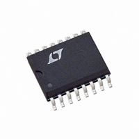
LT1158ISW#TRPBF Linear Technology, LT1158ISW#TRPBF Datasheet - Page 8

LT1158ISW#TRPBF
Manufacturer Part Number
LT1158ISW#TRPBF
Description
IC MOSFET DVR 1/2BRDG NCH 16SOIC
Manufacturer
Linear Technology
Datasheet
1.LT1158CNPBF.pdf
(22 pages)
Specifications of LT1158ISW#TRPBF
Configuration
Half Bridge
Input Type
PWM
Current - Peak
500mA
Number Of Configurations
1
Number Of Outputs
2
High Side Voltage - Max (bootstrap)
56V
Voltage - Supply
5 V ~ 30 V
Operating Temperature
-40°C ~ 85°C
Mounting Type
Surface Mount
Package / Case
16-SOIC (0.300", 7.5mm Width)
Lead Free Status / RoHS Status
Lead free / RoHS Compliant
Delay Time
-
Available stocks
Company
Part Number
Manufacturer
Quantity
Price
LT1158
TEST CIRCUIT
OPERATION
The LT1158 self-enables via an internal 25μA pull-up on
the enable pin 4. When pin 4 is pulled down, much of the
input logic is disabled, reducing supply current to 2mA.
With pin 4 low, the input state is ignored and both MOSFET
gates are actively held low. With pin 4 enabled, one or the
other of the 2 MOSFETs is turned on, depending on the
state of the input pin 6: high for top side on, and low for
bottom side on. The 1.4V input threshold is regulated and
has 200mV of hysteresis.
In order to allow operation over 5V to 30V nominal supply
voltages, an internal bias generator is employed to furnish
constant bias voltages and currents. The bias generator is
decoupled at pin 3 to eliminate any effects from switching
transients. No DC loading is allowed on pin 3.
The top and bottom gate drivers in the LT1158 each utilize
two gate connections: 1) A gate drive pin, which provides
the turn-on and turn-off currents through an optional series
gate resistor; and 2) A gate feedback pin which connects
directly to the gate to monitor the gate-to-source voltage
and supply the DC gate sustaining current.
8
V4
V
V6
+
+
+
+
(Refer to Functional Diagram)
50Ω
10μF
150Ω
2W
1/2W
3k
0.01μF
1
2
3
4
5
6
7
8
BOOST DR
V
BIAS
ENABLE
FAULT
INPUT
GND
B GATE FB
+
LT1158
B GATE DR
T GATE DR
T GATE FB
T SOURCE
SENSE
SENSE
BOOST
V
+
–
+
16
15
14
13
12
11
10
9
+
Whenever there is an input transition on pin 6, the LT1158
follows a logical sequence to turn off one MOSFET and turn
on the other. First, turn-off is initiated, then V
tored until it has decreased below the turn-off threshold,
and fi nally the other gate is turned on. An input latch gets
reset by every low state at pin 6, but can only be set if the
top source pin has gone low, indicating that there will be
suffi cient charge in the bootstrap capacitor to safely turn
on the top MOSFET.
In order to conserve power, the gate drivers only provide
turn-on current for up to 2μs, set by internal one-shot
circuits. Each LT1158 driver can deliver 500mA for 2μs,
or 1000nC of gate charge––more than enough to turn on
multiple MOSFETs in parallel. Once turned on, each gate
is held high by a DC gate sustaining current: the bottom
gate by a 100μA current source, and the top gate by an
on-chip charge pump running at approximately 500kHz.
The fl oating supply for the top side driver is provided by
a bootstrap capacitor between the boost pin 16 and top
source pin 13. This capacitor is recharged each time pin 13
V8
3000pF
100Ω
+
V14 – V13
+
+
1μF
3000pF
V11
VN2222LL
+
2k
1/2W
LT1158 TC01
V12
CLOSED
LOOP
+
V16
GS
is moni-
1158fb


