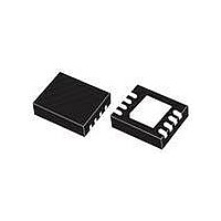
L6747CTR STMicroelectronics, L6747CTR Datasheet - Page 10

L6747CTR
Manufacturer Part Number
L6747CTR
Description
IC MOSFET DVR N-CH DUAL 8-VFDFPN
Manufacturer
STMicroelectronics
Type
High Current MOSFET Driverr
Datasheet
1.L6747CTR.pdf
(15 pages)
Specifications of L6747CTR
Configuration
High and Low Side, Synchronous
Input Type
PWM
Delay Time
30ns
Current - Peak
3.5A
Number Of Configurations
1
Number Of Outputs
2
High Side Voltage - Max (bootstrap)
41V
Voltage - Supply
5 V ~ 12 V
Operating Temperature
0°C ~ 70°C
Mounting Type
Surface Mount
Package / Case
*
Product
MOSFET Gate Drivers
Propagation Delay Time
45 ns
Supply Voltage (max)
12 V
Supply Voltage (min)
5 V
Supply Current
3.5 mA
Maximum Power Dissipation
2.25 W
Maximum Operating Temperature
+ 125 C
Mounting Style
SMD/SMT
Minimum Operating Temperature
0 C
Number Of Drivers
2
Output Current
1 A to 1.5 A
Lead Free Status / RoHS Status
Lead free / RoHS Compliant
Other names
497-10612-2
Device description and operation
4.4
10/15
To prevent the bootstrap capacitor from overcharging as a consequence of large negative
spikes, an external series R
series with the BOOT pin.
Figure 5.
Power dissipation
The L6747C embeds high current drivers for both high-side and low-side MOSFETs. It is
therefore important to consider the power that the device is going to dissipate in driving
them in order to avoid exceeding the maximum junction operating temperature.
Two main factors contribute to device power dissipation: bias power and driver power.
●
●
The total power dissipated to switch the MOSFETs is:
When designing an application based on the L6747C it is recommended to take into
consideration the effect of external gate resistors on the power dissipated by the driver.
External gate resistors help the device to dissipate the switching power since the same
power P
resulting in a general cooling of the device.
Referring to
stage with two different MOSFETs: a P-MOSFET to drive the external gate high, and an N-
MOSFET to drive the external gate low (with their own R
R
(C
lo_LS
G_HS
2.5
2.0
1.5
1.0
0.5
0.0
0
Device power (P
supply pins and is easily quantifiable as follows:
Driver power is the power needed by the driver to continuously switch the external
MOSFETs ON and OFF. It is a function of the switching frequency and total gate
charge of the selected MOSFETs. It can be quantified considering that the total power
P
gate resistance (when present), intrinsic MOSFET resistance, and intrinsic driver
resistance. This last factor is the important one to be determined to calculate the device
power dissipation.
P
P
SW
). The external power MOSFET can be represented in this case as a capacitance
DC
SW
, C
SW
10
Cboot = 47nF
Cboot = 100nF
Cboot = 220nF
Cboot = 330nF
Cboot = 470nF
=
dissipated to switch the MOSFETs is influenced by three main factors: external
=
G_LS
is shared between the internal driver impedance and the external resistor,
V
20
F
Figure
Bootstrap capacitance design
CC
SW
) that stores the gate-charge (Q
High-Side MOSFET Gate Charge [nC]
30
⋅
⋅
I
(
CC
Q
6, a classic MOSFET driver can be represented by a push-pull output
40
GHS
+
DC
V
50
) depends on the static consumption of the device through the
PVCC
⋅
PVCC
60
BOOT
⋅
Doc ID 17127 Rev 1
I
PVCC
70
+
resistor (in the range of few ohms) may be required in
Q
80
GLS
90
⋅
VCC
100
)
G_HS
2500
2000
1500
1000
500
0
0.0
, Q
G_LS
DS(on)
0.2
) required by the external power
: R
Boot Cap Delta Voltage [V]
hi_HS,
0.4
R
lo_HS
0.6
Qg = 10nC
Qg = 25nC
Qg = 50nC
Qg = 100nC
, R
hi_LS,
0.8
L6747C
1.0


