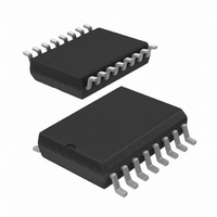
UBA2025T/N1,518 NXP Semiconductors, UBA2025T/N1,518 Datasheet - Page 7

UBA2025T/N1,518
Manufacturer Part Number
UBA2025T/N1,518
Description
IC DRIVER HALF BRIDGE 16-SOIC
Manufacturer
NXP Semiconductors
Type
CFL/TL Driverr
Specifications of UBA2025T/N1,518
Package / Case
16-SOIC (0.300", 7.5mm Width)
Frequency
42.21 ~ 44.59 kHz
Current - Supply
1.6mA
Current - Output
1.5A
Operating Temperature
-40°C ~ 150°C
Driver Type
CFL Drivers
Operating Supply Voltage
600 V
Maximum Operating Temperature
+ 150 C
Mounting Style
SMD/SMT
Maximum Output Current
1.5 A
Minimum Operating Temperature
- 40 C
Supply Current
1.6 mA
Lead Free Status / RoHS Status
Lead free / RoHS Compliant
Voltage - Supply
-
Lead Free Status / Rohs Status
Lead free / RoHS Compliant
Other names
568-4923-2
935287838518
935287838518
NXP Semiconductors
UBA2025_1
Product data sheet
7.12 Frequency and change in frequency
7.13 Ground pins
7.14 Charge coupling
Table 3.
The drive voltage at gate of T2 (G2) will exceed the drive voltage of the high side driver.
At any point in time during oscillation, the circuit will operate between f
change in frequency will be gradual, no steps in frequency will occur. Changes in
frequency caused by a change in voltage at pin CI, show a rather constant df/dt over the
entire frequency range. The following rates are realised (at a frequency of 85 kHz and a
100 nF connected to pin CI):
Pin PGND and pin GND are the ground references of the IC with respect to the
application. Pin SGND provides a local ground reference for the components connected
to pins CPAV, CI, IREF and CF. Other external connections to pin SGND are not preferred.
The sum of currents flowing out of the pins CPAV, CI, IREF, CF and SGND must remain
zero at any time. Pin GND is internally connected to SGND.
Due to parasitic capacitive coupling to the high voltage circuitry, all pins are exposed to a
repetitive charge injection. Given the typical application in figure 6, the pins IREF and CF
are sensitive to this charge injection. For the rating Q
IC is guaranteed, independent of the current level. Charge coupling at current levels below
50 A will not interfere with the accuracy of the V
at current levels below 20 A will not interfere with the accuracy of any parameter.
Frequency
< 75 kHz
75 kHz to 80 kHz
> 85 kHz
•
•
•
For any increase in frequency the df/dt will be between 15 kHz/ms and 37.5 kHz/ms
During preheat and normal operation: the df/dt for a decrease in frequency is between
During the ignition phase: the df/dt for a decrease in frequency is between
6 kHz/ms and 15 kHz/ms
150 Hz/msand 375 Hz/ms.
Minimum gate voltages
Rev. 01 — 16 October 2009
Voltage
8 V (min.)
7 V (min.)
6 V (min.)
th(capm)
coup
and V
a safe functional operation of the
shunt
levels. Charge coupling
UBA2025
btm
© NXP B.V. 2009. All rights reserved.
and f
CFL power IC
start
. Any
7 of 17


