NCL30100SNT1G ON Semiconductor, NCL30100SNT1G Datasheet - Page 9
NCL30100SNT1G
Manufacturer Part Number
NCL30100SNT1G
Description
IC LINEAR
Manufacturer
ON Semiconductor
Specifications of NCL30100SNT1G
Constant Current
*
Constant Voltage
*
Topology
*
Number Of Outputs
*
Internal Driver
*
Type - Primary
*
Type - Secondary
*
Frequency
*
Voltage - Supply
*
Voltage - Output
*
Mounting Type
Surface Mount
Package / Case
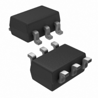
6-TSOP
Operating Temperature
*
Current - Output / Channel
*
Operating Supply Voltage
6.35 V to 18 V
Maximum Operating Temperature
+ 125 C
Mounting Style
SMD/SMT
Minimum Operating Temperature
- 40 C
Led Driver Application
LED Track Lighting, Landscape Lighting, Outdoor Area Lighting
No. Of Outputs
1
Output Current
1.2A
Input Voltage
6.35V To 18V
Dimming Control Type
PWM
Rohs Compliant
Yes
Leaded Process Compatible
Yes
Peak Reflow Compatible (260 C)
Yes
Operating Temperature Range
-40°C To +125°C
Switching Frequency
700kHz
Efficiency
95%
Lead Free Status / RoHS Status
Lead free / RoHS Compliant
Other names
NCL30100SNT1GOSTR
Available stocks
Company
Part Number
Manufacturer
Quantity
Price
Company:

Part Number:
NCL30100SNT1G
Manufacturer:
ON Semiconductor
Quantity:
500


and I3 represent different delays depending on the
magnitude of IVC.
Gate Driver
directly drive a power MOSFET. It features unbalanced
source and sink capabilities to optimize switch on and off
performance without additional external components. The
power MOSFET is switched off at high drain current, to
minimize its switch off losses the sink capability of the gate
driver is increased for a faster switch off. On the other hand,
the source capability of the driver is reduced to slow−down
the power MOSFET at switch on in order to reduce EMI
generation. Whenever the IC supply voltage is lower than
the under voltage threshold, the Gate Driver is low, pulling
down the gate to ground thus eliminating the need for an
external resistor.
Input Voltage Compensation:
optional flexibility to sense the input voltage and modify the
current sense threshold and off time. This function provides
a feed forward mechanism that can be used when the input
voltage of the controller is loosely regulated to improve
output current regulation. If the input voltage is well
regulated, the IVC input can also be used to adjust the offset
of the off time comparator and the current sense control to
achieve the best current regulation accuracy.
supply results in a current being injected into this pin which
has an internal 17 kW resistor connected to a current mirror.
This current information is used to modify V
By changing V
modified and the off time is increased. A small capacitor
should be connected between the IVC pin and ground to
filter out noise generated during switching period. Figure 19
shows the simplified internal schematic:
The Gate Driver consists of a CMOS buffer designed to
The Input Voltage Compensation block gives the user
An external resistor connected between IVC and the input
offset
the off time comparator threshold is
Figure 21. Input Voltage Compensation Loop – Current Sense Control
IVC
17 kW
To Current Sense Comparator
offset
Current
Mirror
4:3
and I
http://onsemi.com
CS
.
9
current) of the input voltage compensation loop control
block can be seen in Figure 20. V
stabilized supply. If no IVC current is injected, the off time
comparator is set to V
This is accomplished by changing the voltage drop on R
The corresponding block diagram of the IVC pin can be seen
in Figure 21.
IVC
The transfer characteristic (output voltage to input
The value of the current injected into IVC also change Ics.
Figure 19. Input Voltage Compensation, OFF Time
37.5 mA
Figure 20. IVC Loop Transfer Characteristic
17 kW
V
V
offset
DD
Current
V
0
Mirror
1:1
IVC Pin Sink Current
offset
12.5 mA
Control
.
CS
Current
Mirror
V
1:1
CC
DD
25 kW
refers to the internal
V
Offset
mA
Comparator
To OFF
Time
shift
.
Related parts for NCL30100SNT1G
Image
Part Number
Description
Manufacturer
Datasheet
Request
R

Part Number:
Description:
Ncl30100 Fixed Off Time Switched Mode Led Driver Controller
Manufacturer:
ON Semiconductor
Datasheet:
Part Number:
Description:
ON Semiconductor [VOLTAGE REGULATOR]
Manufacturer:
ON Semiconductor
Datasheet:
Part Number:
Description:
357-036-542-201 CARDEDGE 36POS DL .156 BLK LOPRO
Manufacturer:
ON Semiconductor
Datasheet:
Part Number:
Description:
357-036-542-201 CARDEDGE 36POS DL .156 BLK LOPRO
Manufacturer:
ON Semiconductor
Datasheet:
Part Number:
Description:
357-036-542-201 CARDEDGE 36POS DL .156 BLK LOPRO
Manufacturer:
ON Semiconductor
Datasheet:
Part Number:
Description:
357-036-542-201 CARDEDGE 36POS DL .156 BLK LOPRO
Manufacturer:
ON Semiconductor
Datasheet:
Part Number:
Description:
357-036-542-201 CARDEDGE 36POS DL .156 BLK LOPRO
Manufacturer:
ON Semiconductor
Datasheet:
Part Number:
Description:
357-036-542-201 CARDEDGE 36POS DL .156 BLK LOPRO
Manufacturer:
ON Semiconductor
Datasheet:
Part Number:
Description:
357-036-542-201 CARDEDGE 36POS DL .156 BLK LOPRO
Manufacturer:
ON Semiconductor
Datasheet:
Part Number:
Description:
357-036-542-201 CARDEDGE 36POS DL .156 BLK LOPRO
Manufacturer:
ON Semiconductor
Datasheet:
Part Number:
Description:
357-036-542-201 CARDEDGE 36POS DL .156 BLK LOPRO
Manufacturer:
ON Semiconductor
Datasheet:
Part Number:
Description:
357-036-542-201 CARDEDGE 36POS DL .156 BLK LOPRO
Manufacturer:
ON Semiconductor
Datasheet:
Part Number:
Description:
Manufacturer:
ON Semiconductor
Datasheet:
Part Number:
Description:
Manufacturer:
ON Semiconductor
Datasheet: