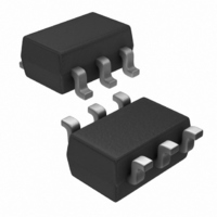
NCL30100SNT1G ON Semiconductor, NCL30100SNT1G Datasheet - Page 7

NCL30100SNT1G
Manufacturer Part Number
NCL30100SNT1G
Description
IC LINEAR
Manufacturer
ON Semiconductor
Specifications of NCL30100SNT1G
Constant Current
*
Constant Voltage
*
Topology
*
Number Of Outputs
*
Internal Driver
*
Type - Primary
*
Type - Secondary
*
Frequency
*
Voltage - Supply
*
Voltage - Output
*
Mounting Type
Surface Mount
Package / Case
6-TSOP
Operating Temperature
*
Current - Output / Channel
*
Operating Supply Voltage
6.35 V to 18 V
Maximum Operating Temperature
+ 125 C
Mounting Style
SMD/SMT
Minimum Operating Temperature
- 40 C
Led Driver Application
LED Track Lighting, Landscape Lighting, Outdoor Area Lighting
No. Of Outputs
1
Output Current
1.2A
Input Voltage
6.35V To 18V
Dimming Control Type
PWM
Rohs Compliant
Yes
Leaded Process Compatible
Yes
Peak Reflow Compatible (260 C)
Yes
Operating Temperature Range
-40°C To +125°C
Switching Frequency
700kHz
Efficiency
95%
Lead Free Status / RoHS Status
Lead free / RoHS Compliant
Other names
NCL30100SNT1GOSTR
Available stocks
Company
Part Number
Manufacturer
Quantity
Price
Company:
Part Number:
NCL30100SNT1G
Manufacturer:
ON Semiconductor
Quantity:
500
scheme with a quasi−fixed OFF time. An optional input
feedforward voltage control is provided to enhance
regulation response with widely varying input voltages.
Only a few external components are necessary to implement
the buck converter. The NCL30100 incorporates the
following features:
•
•
•
•
•
The following section describes in detail each of the control
blocks
Current Sensing Block
current sensing which is used to set the peak current through
The NCL30100 implements a peak current mode control
The NCL30100 utilizes a technique called negative
Very Low Startup Current: The patented internal supply
block is specially designed to offer a very low current
consumption during startup.
Negative Current Sensing: By sensing the total current,
this technique does not impact the MOSFET driving
voltage (V
programming resistor together with the pin capacitance
forms a residual noise filter which blanks spurious
spikes. This approach also supports a flexible resistor
selection. Finally unlike a positive sensing approach,
there is virtually no power dissipation in the current
sense resistor thus improving efficiency.
Controller architecture supports high brightness LED
drive current requirements: Selection of the external
n−channel MOSFET can be easily optimized based on
operation voltage, drive current and size giving the
designer flexibility to easily make design tradeoffs.
Typical $5.5% Current Regulation: The I
$5.5% from 0 to 85°C (+5.5% −9.5% across −40°C to
125°C) accuracy of the current typically, so the LED
peak current is precisely controlled
No output capacitor is needed: By operating the
controller in continuous conduction mode, it is possible
to eliminate the bulky output filter capacitor.
GS
) during switching. Furthermore, the
APPLICATION INFORMATION
CS
pin offers
http://onsemi.com
7
the switch and the inductor. This approach offers several
benefits over traditional positive current sensing.
•
•
•
•
The current sensing circuit is shown in Figure 15.
Maximum peak voltage across the current sense resistor
is user controlled and can be optimized by changing the
value of the shift resistor.
The gate drive capability is improved because the
current sense resistor is located out of the gate driver
loop and does not deteriorate the switch on and also
switch off gate drive amplitude.
Natural leading edge blanking is filter switching noise
at FET turn−in
The CS pin is not exposed to negative voltage, which
could induce a parasitic substrate current within the IC
and distort the surrounding internal circuitry.
V
shift
Figure 15. Primary Current Sensing
R
IVC
CS
shift
R
V
CS
CS
GND
Input Voltage
I
primary
12.5−50 mA
Regulator
To Latch


