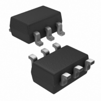
NCL30100SNT1G ON Semiconductor, NCL30100SNT1G Datasheet - Page 15

NCL30100SNT1G
Manufacturer Part Number
NCL30100SNT1G
Description
IC LINEAR
Manufacturer
ON Semiconductor
Specifications of NCL30100SNT1G
Constant Current
*
Constant Voltage
*
Topology
*
Number Of Outputs
*
Internal Driver
*
Type - Primary
*
Type - Secondary
*
Frequency
*
Voltage - Supply
*
Voltage - Output
*
Mounting Type
Surface Mount
Package / Case
6-TSOP
Operating Temperature
*
Current - Output / Channel
*
Operating Supply Voltage
6.35 V to 18 V
Maximum Operating Temperature
+ 125 C
Mounting Style
SMD/SMT
Minimum Operating Temperature
- 40 C
Led Driver Application
LED Track Lighting, Landscape Lighting, Outdoor Area Lighting
No. Of Outputs
1
Output Current
1.2A
Input Voltage
6.35V To 18V
Dimming Control Type
PWM
Rohs Compliant
Yes
Leaded Process Compatible
Yes
Peak Reflow Compatible (260 C)
Yes
Operating Temperature Range
-40°C To +125°C
Switching Frequency
700kHz
Efficiency
95%
Lead Free Status / RoHS Status
Lead free / RoHS Compliant
Other names
NCL30100SNT1GOSTR
Available stocks
Company
Part Number
Manufacturer
Quantity
Price
Company:
Part Number:
NCL30100SNT1G
Manufacturer:
ON Semiconductor
Quantity:
500
the internal propagation delay so the current overshoot from
target is approximately 40 mA as calculated in Equation 18.
R
2.7 kW and 30 kW.
calculate the die power dissipation:
V +
shift
R
P
V/L is simply the slew rate through the inductor and t
All values necessary for R
This value of resistance can be a parallel combination of
To understand the operating junction temperature, we
DIE
shift
^ 0.0402 A
I
I
LED
LED
value is described by this formula:
di @ L
+ V
+ 12 @ 300 @ 10
+ 39.8 mW
+
+
dt
R
0.1 @ ( 0.76 * 0.0402 ) ) 0.038
CC
sense
å I
Figure 28. A Current Error Between the Intended Peak Current and the Actual Peak Current
@ 300 @ 10
delay
@ I
(V
(V
44.07 @ 10
in
in
pk
+
-V
-V
L
L
I
* I
CS
t
t
V @ t
−6
I
I
I
I
on
on
LED
LED
peak
peak
cs
cs
L
−6
delay
) 560 @ 10
) C
shift
)
)
+
−6
8.8 @ 215 @ 10
) V
t
t
calculation are known, the
MOSFET
d
d
47 @ 10
th
−12
@ V
^ 2496 W
@ 12 @ 450 @ 10
−6
CC
−9
@ f
switching
(eq. 18)
(eq. 19)
(eq. 20)
-V
-V
-V
http://onsemi.com
LED
LED
LED
d
t
t
3
off
off
is
- V
- V
- V
L
L
L
15
diode
diode
diode
Using the P
components necessary for a specific set of operating
conditions
ON Semiconductor website.
line. Since Capacitor C3 is charged from a sinusoidal
voltage. If the input voltage approaches zero, the IC is still
supplied from C3. Due to this diode, the IC keeps the LED
driver operating even if the sinusoidal voltage is lower than
V
make sense only if a single LED is used and the converter is
supplied by sinusoidal voltage 12 Vac. For two LEDs in
series their forward voltage is almost as high as V
the IC.
applications which will have an influence on the circuit
operation. They are depending on the PCB design which is
user dependent. The BOM, PCB and some plots are enclosed
for better understanding of the system behavior.
Temp
CC(min)
A design spreadsheet to aid in calculating the external
For a low voltage AC input diode D3 is placed into the Vcc
Parasitic capacitance and inductance are presented in real
IC
until V
+ T
+ T
DIE
is
A
A
, we can calculate junction temperature:
) P
) 7.1° C
in
is lower than V
available
DIE
@ R
qJA
+ T
for
LED
A
) 0.0399 @ 178
. The use of this diode
download
Δi
L
CC(min)
at
(eq. 21)
the
of


