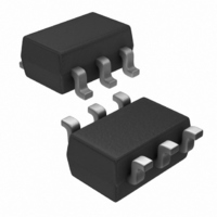
NCL30100SNT1G ON Semiconductor, NCL30100SNT1G Datasheet
NCL30100SNT1G
Specifications of NCL30100SNT1G
Available stocks


Related parts for NCL30100SNT1G

NCL30100SNT1G Summary of contents
Page 1
... PIN CONNECTIONS CS 1 GND (Top View) ORDERING INFORMATION Device Package NCL30100SNT1G TSOP−6 (Pb−Free) †For information on tape and reel specifications, including part orientation and tape sizes, please refer to our Tape and Reel Packaging Specifications Brochure, BRD8011/D. 1 Publication Order Number: MARKING DIAGRAM ...
Page 2
− R4 Figure 1. Typical Application Example of the LED Converter PIN FUNCTION DESCRIPTION Pin N5 Pin Name Function 1 CS Current sense input 2 GND Ground 3 C Timing capacitor T 4 ...
Page 3
Input Voltage IVC Regulator 12.5−50 mA GND Current Sense Comparator MAXIMUM RATINGS Rating Power Supply Voltage IVC Pins Voltage Range CS and C Pin Voltage Range T Thermal Resistance, Junction−to−Air Junction Temperature Storage Temperature Range ESD ...
Page 4
ELECTRICAL CHARACTERISTICS otherwise noted) SUPPLY SECTION Parameter INPUT VOLTAGE COMPENSATION Offset Voltage C Pin Voltage T C Pin Voltage T IVC pin internal resistance (Note 4) C PIN – OFF TIME CONTROL T Source Current Source Current Source Current Maximum ...
Page 5
TEMPERATURE (°C) Figure 3. V Threshold vs. Junction startup Temperature 12.6 12.5 12.4 12.3 12.2 12.1 12.0 11.9 11.8 11.7 11.6 −40 − TEMPERATURE ...
Page 6
TEMPERATURE (°C) Figure 9. Comparator Threshold Voltage vs. Junction Temperature −40 − ...
Page 7
The NCL30100 implements a peak current mode control scheme with a quasi−fixed OFF time. An optional input feedforward voltage control is provided to enhance regulation response with widely varying input voltages. Only a few external components are necessary to implement ...
Page 8
Once the external MOSFET is switched on, the inductor current starts to flow through the sense resistor R current creates a voltage drop V on the resistor negative with respect to GND. Since the comparator connected to ...
Page 9
I3 represent different delays depending on the magnitude of IVC. Gate Driver The Gate Driver consists of a CMOS buffer designed to directly drive a power MOSFET. It features unbalanced source and sink capabilities to optimize switch on and ...
Page 10
The current sense characteristic can be seen in Figure 22. As illustrated, by varied the IVC current between 0 − 50 mA, the sourcing current can range from Figure ...
Page 11
Reverse Buck Operating Description Figure 23 illustrates a typical application schematic and Figure 24 displays simplified waveforms illustrate the converter in steady state operation for critical circuit nodes. Vin Imag IC1 ICS NCL30100 DRV 2 Rshift 5 ...
Page 12
Vcc V DRV 0 Ipk I mag 0 I demag Imin 0 I LED Sense Figure 24. Voltage and Current Nodes ...
Page 13
Application Design Example: A typical step down application will be used to illustrate the basic design process based on nominal design parameters: • Input voltage: V • Nominal LED current: 700 mA (rms) • LED : 120 mA (peak−to−peak) ripple ...
Page 14
Rivc = 300k 500 Rivc = 510k 400 Rivc = 1 Meg Rivc = 1.5 Meg 300 Rivc = 2.2 Meg 200 Rivc = 3.7 Meg Rivc = infinity 100 ...
Page 15
... A design spreadsheet to aid in calculating the external components necessary for a specific set of operating conditions ON Semiconductor website. For a low voltage AC input diode D3 is placed into the Vcc line. Since Capacitor C3 is charged from a sinusoidal voltage. If the input voltage approaches zero, the IC is still supplied from C3 ...
Page 16
... Part Number Allowed Pb−Free 08053C225KAT2A Yes Yes Yes Yes 08053D475KAT2A Yes Yes Yes Yes MBR130T3G No Yes MMSZ16T1G No Yes NSR0520V2T1G No Yes NSR0340HT1G No Yes NCL30100SNT1G No Yes 744774147 No Yes NTGS4141NT1G No Yes NTF3055−100T1G No Yes NTD23N03RT4G No Yes NTJS4160NT1G No Yes NTR4170NT1G No Yes BC817−16LT1G No Yes Com- ...
Page 17
... Resistor 0 Resistor 2 Resistor Resistor 5.6 k Figure 32. Snapshot of CT Pin Voltage, Driver and ILED Tol Footprint Manufacturer − SOT−23 ON semiconductors 1% 0603 Rohm Semiconductor MCR03EZPFX1504 1% 0603 Rohm Semiconductor MCR03EZPFX3000 1% 0603 Rohm Semiconductor MCR03EZPFX3002 1% 0805 Welwyn LRCS0805−0R1FT5 1% 0603 Rohm Semiconductor MCR03EZPFX2701 1% 0603 ...
Page 18
Figure 34. Current Through LED if 50% Dimming at 1 kHz is Applied Figures 36 and 37 illustrate leading edge and trailing edge waveforms from a chopped AC source. For proper dimming control, the bulk capacitance must be reduced to ...
Page 19
Figure 38. ILED and Vin Waveform if No Dimming is Used 84 DC Voltage Efficiency (No Bridge Rectifier INPUT VOLTAGE (V) Figure 39. Efficiency Measurement for the ...
Page 20
Figure 42. PCB Top Side MR 16 Application Figure 43. PCB Top Side Devices Placement D7 R1 NCL30100 R3 CS DRV R5 GND VCC CT IVC Figure ...
Page 21
Figure 45. PCB Bottom Side Devices Placement Figure 46. Top Side Photo Figure 47. Bottom Side Photo http://onsemi.com 21 ...
Page 22
... Pb−Free 08053C225KAT2A Yes Yes C0603C330J5GACTU Yes Yes 08053D475KAT2A Yes Yes C0603C104K5RACTU Yes Yes MBR130T3G No Yes MM5Z16VT1G No Yes NSR0340HT1G No Yes NSR0520V2T1G No Yes NCL30100SNT1G No Yes 744774147 No Yes NTGS4141NT1G No Yes NTF3055−100T1G No Yes NTJS4160NT1G No Yes NTR4170NT1G No Yes MCR03EZPFX1504 Yes Yes MCR03EZPFX3000 Yes Yes MCR03EZPFX3002 ...
Page 23
D1 L1 MRA4003 Vac 100u CX1 D3 MRA4003 2.2n D4 MRA4003 Vac D6 MRA4003 DIMM 0/5 V Figure 48. Design Example Schematic of 115 Vac Converter The input voltage in range 85−140 Vac is rectified by bridge rectifier D1, D3, ...
Page 24
Figure 51. ILED and V Waveform in Figure 52. ILED at the Peak of Sinusoidal Voltage http://onsemi.com 24 ...
Page 25
Figure 53. Input Voltage and Input Current http://onsemi.com 25 ...
Page 26
... Allowed Pb−Free Yes Yes Yes Yes Yes Yes Yes Yes 08053D105KAT2A Yes Yes MRA4003T3G No Yes MURA130T3G No Yes MMSD4148T1G No Yes MMSZ16VT1G No Yes NCL30100SNT1G No Yes 7445620 No Yes 7447709102 No Yes MTD6N20ET4G No Yes BC817−16LT1G No Yes NTS4001NT1G No Yes MCR06EZPFX2402 Yes Yes MCR03EZPFX1503 Yes Yes MCR03EZPFX5601 ...
Page 27
... A 0.05 A1 *For additional information on our Pb−Free strategy and soldering details, please download the ON Semiconductor Soldering and Mounting Techniques Reference Manual, SOLDERRM/D. ON Semiconductor and are registered trademarks of Semiconductor Components Industries, LLC (SCILLC). SCILLC reserves the right to make changes without further notice to any products herein. SCILLC makes no warranty, representation or guarantee regarding the suitability of its products for any particular purpose, nor does SCILLC assume any liability arising out of the application or use of any product or circuit, and specifically disclaims any and all liability, including without limitation special, consequential or incidental damages. “ ...