CY8CLEDAC02 Cypress Semiconductor Corp, CY8CLEDAC02 Datasheet - Page 8

CY8CLEDAC02
Manufacturer Part Number
CY8CLEDAC02
Description
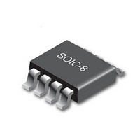
IC CTLR AC-DC DIMMABLE LED 8SOIC
Manufacturer
Cypress Semiconductor Corp
Type
High Power, AC Input, Dimmabler
Datasheet
1.CY8CLEDAC02.pdf
(20 pages)
Specifications of CY8CLEDAC02
Package / Case
8-SOIC (3.9mm Width)
Voltage - Supply
8 V ~ 16 V
Frequency
200kHz
Operating Temperature
-40°C ~ 85°C
Number Of Outputs
1
Internal Switch(s)
No
Efficiency
85%
Topology
AC DC Offline Switcher
Operating Supply Voltage
- 0.3 V to 18 V
Maximum Supply Current
20 mA
Maximum Power Dissipation
526 mW
Maximum Operating Temperature
+ 85 C
Mounting Style
SMD/SMT
Minimum Operating Temperature
- 40 C
Operating Temperature (min)
-40C
Operating Temperature (max)
85C
Operating Temperature Classification
Industrial
Pin Count
8
Mounting
Surface Mount
Operating Supply Voltage (max)
18V
Lead Free Status / RoHS Status
Lead free / RoHS Compliant
Voltage - Output
-
Current - Output / Channel
-
Lead Free Status / Rohs Status
Lead free / RoHS Compliant
Available stocks
Company
Part Number
Manufacturer
Quantity
Price
Company:
Part Number:
CY8CLEDAC02
Manufacturer:
TI
Quantity:
900
Part Number:
CY8CLEDAC02
Manufacturer:
CYPRESS/赛普拉斯
Quantity:
20 000
Chopping Operation
The chopping circuit provides four key functions:
■
■
■
■
The chopping circuit is shown in
short on pulses, the circuit operates as a boost converter. When
Q2 turns on, the chopping inductor L3 stores energy. When Q2
turns off, this energy is released to capacitor C3 through diode
D3. Source resistor R6 is used to limit the current in the chopper
path to optimize the efficiency of the circuit. A dithering algorithm
is used to control the period for Q2 to minimize EMI generated
by the mainly discontinuous operation of the boost circuit. The
voltage on Z
only available internal to the device.
During the chopping period, the average current in L3 is in phase
with and proportional to the input mains voltage inherently gener-
ating high power factor.
If the circuit determines it is connected to a dimmer, Q2 is held
on while the mains voltage in is low. This provides a load on the
dimmer enabling the internal circuitry of the dimmer to reset
correctly for each half cycle. For leading edge dimmers, Q2 is
held on for a significant time after the triac in the dimmer fires
each half cycle. During this period L3 will saturate and R6
provides the current necessary for the triac latch current to be
reached. For trailing edge dimmers, Q2 is held high after the
trailing edge. This load forces the line to quickly fall to zero when
Document Number: 001-54879 Rev. *C
At startup, it provides a low impedance load on the wall dimmer
enabling the type of dimmer (none, leading edge, or trailing
edge) to be determined.
Each cycle intelligently provides a low impedance load to:
❐
❐
Improves Power Factor
Minimizes mains cycle peak current for triac based (leading
edge) dimmers by boosting energy into the bulk capacitor.
Enable accurate determination of mains zero crossing points.
Meet triac trigger current and latch current requirements for
triac based (leading edge) dimmers.
AC
VIN
is the scaled rectified mains voltage, a voltage
DIMMER
WALL
F1
Figure
R2
L1
L2
R1
8. When Q2 is driven with
C1
Figure 8. Chopper Circuit
AC
AC
BR1
D8
D9
+
_
the dimmer turns off, enabling accurate detection of the dimmer
on time.
D8 and D9 ensure C3 is charged to peak voltage output from the
dimmer. This maximizes the voltage on C3 each half cycle,
minimizing the in rush current when the triac fires on the next half
cycle.
The chopper operates in three different modes as follows:
■
■
■
Figure 7. Chopping Operation (No Dimmer Mode)
R3 + R4
V
No dimmer: Chopper operates when the internal voltage at Z
is above a pre-defined chopping threshold. The chopper
remains off otherwise.(see
Leading edge dimmer mode: The chopping period is defined
as the percentage of the dimming period (T
chopper FET remains hard on during the zero crossing section
on V
Trailing edge dimmer mode: Chopping circuit is active across
the entire dimming period (T
hard on otherwise (see
IN
(Internal)
(pin)
Z
VIN
IN
.(see
D1
Figure
C2
L3
9)
Q2
Figure
R5
R6
Figure
CROSS
D3
BOOST (pin)
10).
). The chopper FET remains
7)
CY8CLEDAC02
CROSS
C3
Page 8 of 20
). The
V
CBULK
VIN
[+] Feedback


