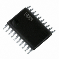
PCA9634PW,118 NXP Semiconductors, PCA9634PW,118 Datasheet - Page 14

PCA9634PW,118
Manufacturer Part Number
PCA9634PW,118
Description
IC LED DRIVER RGBA 20-TSSOP
Manufacturer
NXP Semiconductors
Type
RGBA LED Driverr
Datasheet
1.PCA9634D118.pdf
(38 pages)
Specifications of PCA9634PW,118
Package / Case
20-TSSOP
Topology
Open Drain, PWM
Number Of Outputs
8
Internal Driver
Yes
Type - Primary
Backlight, LED Blinker
Type - Secondary
RGBA
Frequency
1MHz
Voltage - Supply
2.3 V ~ 5.5 V
Voltage - Output
5.5V
Mounting Type
Surface Mount
Operating Temperature
-40°C ~ 85°C
Current - Output / Channel
25mA
Internal Switch(s)
Yes
Low Level Output Current
25 mA
High Level Output Current
50 uA
Operating Supply Voltage
2.3 V to 5.5 V
Maximum Supply Current
10 mA
Maximum Power Dissipation
400 mW
Maximum Operating Temperature
+ 85 C
Mounting Style
SMD/SMT
Minimum Operating Temperature
- 40 C
Lead Free Status / RoHS Status
Lead free / RoHS Compliant
Efficiency
-
Lead Free Status / Rohs Status
Lead free / RoHS Compliant
Other names
568-4066-2
935282233118
PCA9634PW-T
PCA9634PW-T
935282233118
PCA9634PW-T
PCA9634PW-T
NXP Semiconductors
PCA9634_6
Product data sheet
7.3.6 LEDOUT0 and LEDOUT1: LED driver output state
7.3.7 SUBADR1 to SUBADR3: I
Table 10.
Legend: * default value.
LDRx = 00 — LED driver x is off (default power-up state).
LDRx = 01 — LED driver x is fully on (individual brightness and group dimming/blinking
not controlled).
LDRx = 10 — LED driver x individual brightness can be controlled through its PWMx
register.
LDRx = 11 — LED driver x individual brightness and group dimming/blinking can be
controlled through its PWMx register and the GRPPWM registers.
Table 11.
Legend: * default value.
Subaddresses are programmable through the I
E4h, E8h, and the device(s) will not acknowledge these addresses right after power-up
(the corresponding SUBx bit in MODE1 register is equal to 0).
Once subaddresses have been programmed to their right values, SUBx bits need to be
set to 1 in order to have the device acknowledging these addresses (MODE1 register).
Only the 7 MSBs representing the I
register is a read-only bit (0).
When SUBx is set to 1, the corresponding I
an I
Address
0Ch
0Dh
Address
0Eh
0Fh
10h
2
C-bus read or write sequence.
Register
SUBADR1
SUBADR2
SUBADR3
LEDOUT0 and LEDOUT1- LED driver output state registers (address 0Ch and
0Dh) bit description
Register
LEDOUT0
LEDOUT1
SUBADR1 to SUBADR3 - I
10h) bit description
Rev. 06 — 12 September 2008
Bit
7:6
5:4
3:2
1:0
7:6
5:4
3:2
1:0
Bit
7:1
0
7:1
0
7:1
0
Symbol
LDR3
LDR2
LDR1
LDR0
LDR7
LDR6
LDR5
LDR4
2
C-bus subaddress 1 to 3
Symbol
A1[7:1]
A1[0]
A2[7:1]
A2[0]
A3[7:1]
A3[0]
2
2
C-bus subaddress are valid. The LSB in SUBADRx
C-bus subaddress registers 1 to 3 (address 0Eh to
Access Value
R/W
R/W
R/W
R/W
R/W
R/W
R/W
R/W
Access Value
R/W
R only
R/W
R only
R/W
R only
2
C-bus subaddress can be used during either
2
C-bus. Default power-up values are E2h,
00*
00*
00*
00*
00*
00*
00*
00*
1110 001*
0*
1110 010*
0*
1110 100*
0*
8-bit Fm+ I
Description
LED3 output state control
LED2 output state control
LED1 output state control
LED0 output state control
LED7 output state control
LED6 output state control
LED5 output state control
LED4 output state control
Description
I
reserved
I
reserved
I
reserved
2
2
2
C-bus subaddress 1
C-bus subaddress 2
C-bus subaddress 3
PCA9634
2
© NXP B.V. 2008. All rights reserved.
C-bus LED driver
14 of 38


