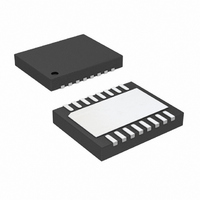
LTC3783EDHD#TRPBF Linear Technology, LTC3783EDHD#TRPBF Datasheet - Page 7

LTC3783EDHD#TRPBF
Manufacturer Part Number
LTC3783EDHD#TRPBF
Description
IC LED DRIVER PWM CONTROL 16-DFN
Manufacturer
Linear Technology
Type
PWM Controlr
Datasheet
1.LTC3783EFEPBF.pdf
(24 pages)
Specifications of LTC3783EDHD#TRPBF
Constant Current
Yes
Constant Voltage
Yes
Topology
Flyback, PWM, SEPIC, Step-Down (Buck), Step-Up (Boost)
Number Of Outputs
1
Internal Driver
No
Type - Primary
Automotive, General Purpose
Frequency
20kHz ~ 1MHz
Voltage - Supply
3 V ~ 36 V
Mounting Type
Surface Mount
Package / Case
16-DFN
Operating Temperature
-40°C ~ 85°C
Internal Switch(s)
No
Lead Free Status / RoHS Status
Lead free / RoHS Compliant
Voltage - Output
-
Current - Output / Channel
-
Efficiency
-
Available stocks
Company
Part Number
Manufacturer
Quantity
Price
PIN FUNCTIONS
FBN (Pin 1): Error Amplifi er Inverting Input/Negative Cur-
rent Sense Pin. In voltage mode (V
senses feedback voltage from either the external resistor
divider across V
grounded sense resistor under the load for output current
regulation. In constant current/constant voltage mode
(V
current-regulating resistor. Nominal voltage for this pin in
regulation is either V
depending on operational mode (voltage or constant cur-
rent/constant voltage) set by the voltage at V
FBP (Pin 2): Error Amplifi er Noninverting Input/Positive
Current Sense Pin. This pin voltage determines the control
loop’s feedback mode (voltage or constant current/constant
voltage), the threshold of which is approximately 2V. In
voltage mode (V
voltage which the regulated loop will cause FBN to follow.
In constant current/constant voltage mode (V
connect this pin to the positive side of the load current-
sensing resistor. The acceptable input ranges for this pin
are 0V to 1.23V (voltage mode) and 2.5V to 36V (constant
current/constant voltage mode).
I
tor offset voltage (V
regulation (i.e., when V
when V
Nominal voltage range for this pin is 0.1V to 1.23V.
V
version of the internal bandgap voltage, which can be
connected to FBP either directly or with attenuation.
Nominal voltage for this pin is 1.23V. This pin should
never be bypassed by a capacitor to GND. Instead, a 10k
resistor to GND should be used to lower pin impedance
in noisy systems.
FREQ (Pin 5): A resistor from the FREQ pin to ground
programs the operating frequency of the chip. The nominal
voltage at the FREQ pin is 0.615V.
SYNC (Pin 6): This input allows for synchronizing the op-
erating frequency to an external clock and has an internal
100k pull-down resistor.
LIM
REF
FBP
(Pin 3): Current Limit Pin. Sets current sense resis-
(P
> 2.5V), connect this pin to the negative side of the
ILIM
IN
4): Reference Voltage Pin. Provides a buffered
= 1.23V and decreases proportionally with V
FBP
OUT
FBP
≤ V
FBP
for output voltage regulation, or the
FBP
REF
or (V
– V
), this pin represents the desired
> 2.5V). Offset voltage is 100mV
FBN
FBP
) in constant current mode
– 100mV) for V
FBP
≤ V
VREF
ILIM
FBP
FBP
), this pin
.
= 1.23V,
> 2.5V),
ILIM
.
PWMIN (Pin 7): PWM Gate Driver Input. Internal 100k
pull-up resistor. While PWMIN is low, PWMOUT is low,
GATE stops switching and the external I
disconnected, saving the I
PWMOUT (Pin 8): PWM Gate Driver Output. Used for con-
stant current dimming (LED load) or for output disconnect
(step-up power supply).
GATE (Pin 9): Main Gate Driver Output for the Boost
Converter.
INTV
and PWM gate drivers and control circuits are powered
from this voltage. Decouple this pin locally to the IC ground
with a minimum of 4.7μF low ESR ceramic capacitor.
V
to ground.
SENSE (Pin 12): Current Sense Input for the Control Loop.
Connect this pin to the drain of the main power MOSFET
for V
Alternatively, the SENSE pin may be connected to a resistor
in the source of the main power MOSFET. Internal leading-
edge blanking is provided for both sensing methods.
SS (Pin 13): Soft-Start Pin. Provides a 50μA pull-up current,
enabled and reset by RUN, which charges an optional external
capacitor. This voltage ramp translates into a corresponding
current limit ramp through the main MOSFET.
OV/FB (Pin 14): Overvoltage Pin/Voltage Feedback Pin.
In voltage mode (V
V
at which GATE switching is disabled in order to prevent
an overvoltage situation. Nominal threshold voltage for
the OV pin is 1.32V (V
current/voltage mode (V
through a resistor divider and brings the loop into voltage
regulation such that pin voltage approaches V
provided the loop is not regulating the load current (e.g.,
[V
IN
OUT
FBP
(Pin 11): Main Supply Pin. Must be closely decoupled
CC
DS
through a resistor network, sets the output voltage
– V
(Pin 10): Internal 7V Regulator Output. The main
sensing and highest effi ciency for V
FBN
] < 100mV for I
FBP
REF
≤ V
FBP
+ 7%) with 20mV hysteresis. In
TH
REF
> 2.5V), this pin senses V
LIM
state.
), this input, connected to
= 1.23V).
LTC3783
TH
SENSE
REF
network is
= 1.23V,
≤ 36V.
3783fb
7
OUT


