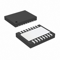
LTC3783EDHD#TRPBF Linear Technology, LTC3783EDHD#TRPBF Datasheet - Page 18

LTC3783EDHD#TRPBF
Manufacturer Part Number
LTC3783EDHD#TRPBF
Description
IC LED DRIVER PWM CONTROL 16-DFN
Manufacturer
Linear Technology
Type
PWM Controlr
Datasheet
1.LTC3783EFEPBF.pdf
(24 pages)
Specifications of LTC3783EDHD#TRPBF
Constant Current
Yes
Constant Voltage
Yes
Topology
Flyback, PWM, SEPIC, Step-Down (Buck), Step-Up (Boost)
Number Of Outputs
1
Internal Driver
No
Type - Primary
Automotive, General Purpose
Frequency
20kHz ~ 1MHz
Voltage - Supply
3 V ~ 36 V
Mounting Type
Surface Mount
Package / Case
16-DFN
Operating Temperature
-40°C ~ 85°C
Internal Switch(s)
No
Lead Free Status / RoHS Status
Lead free / RoHS Compliant
Voltage - Output
-
Current - Output / Channel
-
Efficiency
-
Available stocks
Company
Part Number
Manufacturer
Quantity
Price
LTC3783
OPERATION
For many designs it is possible to choose a single capacitor
type that satisfi es both the ESR and bulk C requirements
for the design. In certain demanding applications, however,
the ripple voltage can be improved signifi cantly by con-
necting two or more types of capacitors in parallel. For
example, using a low ESR ceramic capacitor can minimize
the ESR setup, while an electrolytic capacitor can be used
to supply the required bulk C.
Once the output capacitor ESR and bulk capacitance have
been determined, the overall ripple voltage waveform
should be verifi ed on a dedicated PC board (see Board
Layout section for more information on component place-
ment). Lab breadboards generally suffer from excessive
series inductance (due to inter-component wiring), and
these parasitics can make the switching waveforms look
signifi cantly worse than they would be on a properly
designed PC board.
The output capacitor in a boost regulator experiences
high RMS ripple currents. The RMS output capacitor
ripple current is:
Note that the ripple current ratings from capacitor manu-
facturers are often based on only 2000 hours of life. This
makes it advisable to further derate the capacitor or to
choose a capacitor rated at a higher temperature than
required. Several capacitors may also be placed in parallel
to meet size or height requirements in the design.
Boost Converter: Input Capacitor Selection
The input capacitor of a boost converter is less critical
than the output capacitor, due to the fact that the inductor
is in series with the input, and hence, the input current
waveform is continuous (see Figure 10). The input volt-
age source impedance determines the size of the input
capacitor, which is typically in the range of 10μF to 100μF .
A low ESR capacitor is recommended, although it is not
as critical as for the output capacitor.
18
I
RMS COUT
(
)
;
I
OUT MAX
(
)
•
V
OUT
V
IN MIN
–
(
V
IN MIN
(
) )
)
The RMS input capacitor ripple current for a boost
converter is:
Please note that the input capacitor can see a very high
surge current when a battery is suddenly connected to
the input of the converter, and solid tantalum capacitors
can fail catastrophically under these conditions. Be sure
to specify surge-tested capacitors!
Boost Converter Design Example
The design example given here will be for the circuit shown
in Figure 1. The input voltage is 12V, and the output voltage
is 25V at a maximum load current of 0.7A (1A peak).
1. The duty cycle is:
2. The operating frequency is chosen to be 1MHz to
maximize the PWM dimming range. From Figure 2, the
resistor from the FREQ pin to ground is 6k.
3. An inductor ripple current of 40% of the maximum load
current is chosen, so the peak input current (which is also
the minimum saturation current) is:
The inductor ripple current is:
I
IN PEAK
(
I
D
Δ =
RMS CIN
=
I
L
V
(
)
OUT
=
χ •
V
)
OUT
⎛
⎝ ⎜
Figure 10. Inductor and Input Currents
+
1
; . •
I
I
1
OUT MAX
L
+
0 3
V
−
+
D
χ
2
D
V
(
–
⎞
⎠ ⎟
MAX
D
V
V
•
IN
IN MIN
I
L f
1
OUT MAX
)
(
–
•
=
=
D
25 0 4 12
(
0 4
MAX
)
. •
25 0 4
•
+
D
)
MAX
+
1 0 53
. –
=
−
0 7
1 2
.
.
. •
.
3783 F10
=
1 0 53
=
I
– .
IN
53
0
0 6
.
.
%
7 7
A
=
1 8
.
3783fb
A


