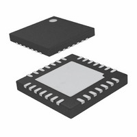
LTC3220IPF-1#PBF Linear Technology, LTC3220IPF-1#PBF Datasheet - Page 8

LTC3220IPF-1#PBF
Manufacturer Part Number
LTC3220IPF-1#PBF
Description
IC LED DRVR QVGA DISPLAY 28UTQFN
Manufacturer
Linear Technology
Type
QVGA Display (I²C Interface)r
Datasheet
1.LTC3220EPFPBF.pdf
(20 pages)
Specifications of LTC3220IPF-1#PBF
Topology
Open Drain, Step-Up (Boost), Switched Capacitor (Charge Pump)
Number Of Outputs
18
Internal Driver
Yes
Type - Primary
Backlight
Type - Secondary
LED Blinker
Frequency
850kHz ~ 1.05MHz
Voltage - Supply
2.9 V ~ 5.5 V
Mounting Type
Surface Mount
Package / Case
28-UTQFN
Operating Temperature
-40°C ~ 125°C
Current - Output / Channel
20mA
Internal Switch(s)
Yes
Efficiency
91%
Lead Free Status / RoHS Status
Lead free / RoHS Compliant
Voltage - Output
-
Available stocks
Company
Part Number
Manufacturer
Quantity
Price
OPERATION
LTC3220/LTC3220-1
Power Management
The LTC3220/LTC3220-1 use a switched capacitor charge
pump to boost CPO as much as 2 times the input voltage
up to 5.1V. The part starts up in 1x mode. In this mode,
V
maximum effi ciency and minimum noise. The LTC3220/
LTC3220-1 will remain in 1x mode until an LED current
source drops out. Dropout occurs when a current source
voltage becomes too low for the programmed current
to be supplied. When dropout is detected, the LTC3220/
LTC3220-1 will switch into 1.5x mode. The CPO voltage
will then start to increase and will attempt to reach 1.5×
V
part to enter the 2x mode. The CPO voltage will attempt
to reach 2× V
A 2-phase non-overlapping clock activates the charge
pump switches. In the 2x mode the fl ying capacitors are
charged on alternate clock phases from V
CPO voltage ripple. In 1.5x mode the fl ying capacitors are
charged in series during the fi rst clock phase and stacked
in parallel on V
of charging and discharging the fl ying capacitors continues
at a constant frequency of 850kHz.
The current delivered by each LED current source is con-
trolled by an associated DAC. Each DAC is programmed
via the I
8
IN
IN
up to 4.6V. Any subsequent dropout will cause the
is connected directly to CPO. This mode provides
2
C port.
IN
IN
up to 5.1V.
during the second phase. This sequence
Figure 1. Charge Pump Open-Loop Thevenin Equivalent Circuit
IN
to minimize
+
–
1.5V
2V
IN
R
IN
OL
OR
3220 F01
Soft-Start
Initially, when the part is in shutdown, a weak switch
connects V
CPO output capacitor and prevent large charging currents
from occurring.
The LTC3220/LTC3220-1 also employ a soft-start feature
on the charge pump to prevent excessive inrush current
and supply droop when switching into the step-up modes.
The current available to the CPO pin is increased linearly
over a typical period of 125μs. Soft-start occurs at the
start of both 1.5x and 2x mode changes.
Charge Pump Strength
When the LTC3220/LTC3220-1 operate in either 1.5x mode
or 2x mode, the charge pump can be modeled as a Theve-
nin-equivalent circuit to determine the amount of current
available from the effective input voltage and effective
open-loop output resistance, R
R
switching term, 1/(2f
tances and the non-overlap period of the switching circuit.
However, for a given R
will be directly proportional to the advantage voltage of
1.5V
Consider the example of driving LEDs from a 3.1V supply.
OL
CPO
IN
is dependent on a number of factors including the
+
–
– CPO for 1.5x mode and 2V
IN
to CPO. This allows V
OSC
OL
, the amount of current available
• C
FLY
OL
), internal switch resis-
(Figure 1).
IN
IN
to slowly charge the
– CPO for 2x mode.
32201fc


