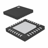
LTC3220IPF-1#PBF Linear Technology, LTC3220IPF-1#PBF Datasheet - Page 11

LTC3220IPF-1#PBF
Manufacturer Part Number
LTC3220IPF-1#PBF
Description
IC LED DRVR QVGA DISPLAY 28UTQFN
Manufacturer
Linear Technology
Type
QVGA Display (I²C Interface)r
Datasheet
1.LTC3220EPFPBF.pdf
(20 pages)
Specifications of LTC3220IPF-1#PBF
Topology
Open Drain, Step-Up (Boost), Switched Capacitor (Charge Pump)
Number Of Outputs
18
Internal Driver
Yes
Type - Primary
Backlight
Type - Secondary
LED Blinker
Frequency
850kHz ~ 1.05MHz
Voltage - Supply
2.9 V ~ 5.5 V
Mounting Type
Surface Mount
Package / Case
28-UTQFN
Operating Temperature
-40°C ~ 125°C
Current - Output / Channel
20mA
Internal Switch(s)
Yes
Efficiency
91%
Lead Free Status / RoHS Status
Lead free / RoHS Compliant
Voltage - Output
-
Available stocks
Company
Part Number
Manufacturer
Quantity
Price
OPERATION
sub-address register is then written to, followed by the
data register. Each data register has a sub-address. After
the data register has been written a load pulse is created
after the stop bit. The load pulse transfers all of the data
held in the data registers to the DAC registers. The stop
bit can be delayed until all of the data master registers
have been written. At this point the LED current will be
changed to the new settings. The serial port uses static
logic registers so there is no minimum speed at which it
can be operated.
I
The LTC3220/LTC3220-1 communicate with a host (master)
using the standard I
(Figure 3) shows the timing relationship of the signals on
the bus. The two bus lines, SDA and SCL, must be high
SDA
SCL
2
START
C Interface
LTC3220
LTC3220-1
0
0
0
1
0
0
0
2
SDA
SCL
t
HD, STA
1
1
1
3
CONDITION
ADDRESS
ADDRESS
2
1
1
1
4
START
C 2-wire interface. The Timing Diagram
1
1
1
5
t
LOW
0
0
0
6
t
0
1
0
7
r
t
HIGH
t
SU, DAT
WR
WR
0
0
0
8
t
ACK
f
9
S7
S7
1
t
HD, DAT
S6
Figure 3. Timing Parameters
S6
2
Figure 2. Bit Assignments
S5
S5
3
SUB-ADDRESS
S4
S4
4
REPEATED START
CONDITION
S3
S3
5
when the bus is not in use. External pull-up resistors or
current sources, such as the LTC1694 SMBus accelerator,
are required on these lines.
The LTC3220/LTC3220-1 are receive-only (slave) devices.
There are two I
address is 0011100 and the LTC3220-1 I
0011101. The I
the LTC3220 and LTC3220-1.
Write Word Protocol Used By the LTC3220/LTC3220-1
S = Start Condition, Wr = Write Bit = 0, A = Acknowledge,
P = Stop Condition
*The sub-address uses only the fi rst 5 bits, D0, D1, D2, D3 and D4.
**Stop can be delayed until all of the data registers have been written.
S2
S2
S Slave Address Wr A *Sub-Address A Data Byte
1
6
t
SU, STA
S1
S1
7
t
HD, STA
S0
S0
8
7
t
SP
ACK
9
2
2
LTC3220/LTC3220-1
C address is the only difference between
C addresses available. The LTC3220 I
7
1
7
1
2
6
1
6
3
5
5
CONDITION
STOP
DATA BYTE
4
4
4
8
t
SU, STO
t
3
5
BUF
3
CONDITION
6
2
2
START
1
3220 F03
7
1
1
2
8
C address is
0
8
0
ACK
9
11
1
A P**
32201fc
STOP
3220 FO2
1
2
C


