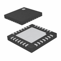
LTC3220IPF-1#PBF Linear Technology, LTC3220IPF-1#PBF Datasheet

LTC3220IPF-1#PBF
Specifications of LTC3220IPF-1#PBF
Available stocks
Related parts for LTC3220IPF-1#PBF
LTC3220IPF-1#PBF Summary of contents
Page 1
... LTC3220/LTC3220-1 into 2x mode. The parts reset to 1x mode whenever a data bit is updated via the I L, LT, LTC and LTM are registered trademarks of Linear Technology Corporation. All other trademarks are the property of their respective owners. Protected by U.S. Patents including 6411531. ...
Page 2
... LTC3220EPF-1#PBF LTC3220EPF-1#TRPBF LTC3220IPF#PBF LTC3220IPF#TRPBF LTC3220IPF-1#PBF LTC3220IPF-1#TRPBF Consult LTC Marketing for parts specifi ed with wider operating temperature ranges. *The temperature grade is identifi label on the shipping container. Consult LTC Marketing for information on non-standard lead based fi nish parts. For more information on lead free part marking, go to: For more information on tape and reel specifi ...
Page 3
ELECTRICAL CHARACTERISTICS temperature range, otherwise specifi cations are at T unless otherwise noted. SYMBOL PARAMETER V Shutdown Current IN DV Shutdown Current CC Universal LED Current, 6-Bit Linear DACs, ULED = 1V Full-Scale LED Current Minimum (I ) LED Current ...
Page 4
LTC3220/LTC3220-1 ELECTRICAL CHARACTERISTICS temperature range, otherwise specifi cations are at T unless otherwise noted. SYMBOL PARAMETER t Data Hold Time HD,DAT(OUT) t Input Data Hold Time HD,DAT(IN) t Data Setup Time SU,DAT t Clock Low Period LOW t Clock High ...
Page 5
TYPICAL PERFORMANCE CHARACTERISTICS 1x Mode Switch Resistance vs Temperature 0.80 0.75 0. 3. 3.6V 0. 3.9V IN 0.50 0.45 0.40 0.35 0.30 –40 –25 – ...
Page 6
LTC3220/LTC3220-1 TYPICAL PERFORMANCE CHARACTERISTICS 1.5x Mode V Current CPO (I – 1.5I ) VIN CPO 120 180 240 300 I (mA) CPO 3220 G13 ULED Current ...
Page 7
PIN FUNCTIONS SDA (Pin 12): Input Data for the Serial Port. Serial data is shifted in one bit per clock cycle to control the LTC3220/ LTC3220-1. The logic level is referenced to DV C1P , C2P , C1M, C2M (Pins ...
Page 8
LTC3220/LTC3220-1 OPERATION Power Management The LTC3220/LTC3220-1 use a switched capacitor charge pump to boost CPO as much as 2 times the input voltage up to 5.1V. The part starts mode. In this mode connected directly ...
Page 9
OPERATION If the LED forward voltage is 3.8V and the current sources require 100mV, the advantage voltage for 1.5x mode is 3.1V • 1.5 – 3.8V – 0.1V or 750mV. Notice that if the input voltage is raised to 3.2V, ...
Page 10
LTC3220/LTC3220-1 OPERATION Blinking Each universal output (ULED1 to ULED18) can be set to blink with an on time of 0.156 seconds, or 0.625 seconds and a period of 1.25 seconds, or 2.5 seconds via the I port. The blinking rate ...
Page 11
OPERATION sub-address register is then written to, followed by the data register. Each data register has a sub-address. After the data register has been written a load pulse is created after the stop bit. The load pulse transfers all of ...
Page 12
LTC3220/LTC3220-1 OPERATION Sub-Address Byte MSB LSB ...
Page 13
OPERATION Data Bytes REG1 to REG18, Universal LED 6-bit linear DAC data with blink/gradation. Sub-Address 00001 to 10010 per Sub-Address Table Blink/Gradation/Dropout Enable Normal Blink Enabled Gradation Enabled GPO Mode* Strong Pull-Down Mode Current Limited Mode High Impedance/Off *(Gradation/Blink/Dropout Off) ...
Page 14
LTC3220/LTC3220-1 OPERATION Bus Speed 2 The I C port is designed to be operated at speeds up to 400kHz. It has built-in timing delays to ensure correct operation when addressed from an I device. It also contains input fi lters ...
Page 15
OPERATION Bus Write Operation The master initiates communication with the LTC3220/ LTC3220-1 with a START condition and a 7-bit address followed by the write bit R the address matches that of the LTC3220/LTC3220-1, the LTC3220/LTC3220-1 return an ...
Page 16
LTC3220/LTC3220-1 APPLICATIONS INFORMATION V , CPO Capacitor Selection IN The style and value of the capacitors used with the LTC3220/ LTC3220-1 determine several important parameters such as regulator control loop stability, output ripple, charge pump strength and minimum start-up time. ...
Page 17
APPLICATIONS INFORMATION Flying Capacitor Selection Warning: Polarized capacitors such as tantalum or aluminum should never be used for the fl ying capaci- tors since their voltage can reverse upon start-up of the LTC3220/LTC3220-1. Ceramic capacitors should always be used for ...
Page 18
LTC3220/LTC3220-1 APPLICATIONS INFORMATION Power Effi ciency To calculate the power effi ciency (η LED driver chip, the LED power should be compared to the input power. The difference between these two numbers represents lost power whether it is ...
Page 19
... ON THE TOP AND BOTTOM OF PACKAGE Information furnished by Linear Technology Corporation is believed to be accurate and reliable. However, no responsibility is assumed for its use. Linear Technology Corporation makes no representa- tion that the interconnection of its circuits as described herein will not infringe on existing patent rights. PF Package 28-Lead UTQFN (4mm × ...
Page 20
... DFN Package 5.5V 300μA, I < 2.5μA, DFN Package 5.25V 25μA/50μA, I <1μ 5.25V 28μA, I <1μA, DFN Package 2.7V to 4.5V 2.5mA, I < 6μA, IN(MAX 0409 REV C • PRINTED IN USA © LINEAR TECHNOLOGY CORPORATION 2007 100k GPO4 32201fc ...


