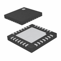
LTC3220IPF-1#PBF Linear Technology, LTC3220IPF-1#PBF Datasheet - Page 14

LTC3220IPF-1#PBF
Manufacturer Part Number
LTC3220IPF-1#PBF
Description
IC LED DRVR QVGA DISPLAY 28UTQFN
Manufacturer
Linear Technology
Type
QVGA Display (I²C Interface)r
Datasheet
1.LTC3220EPFPBF.pdf
(20 pages)
Specifications of LTC3220IPF-1#PBF
Topology
Open Drain, Step-Up (Boost), Switched Capacitor (Charge Pump)
Number Of Outputs
18
Internal Driver
Yes
Type - Primary
Backlight
Type - Secondary
LED Blinker
Frequency
850kHz ~ 1.05MHz
Voltage - Supply
2.9 V ~ 5.5 V
Mounting Type
Surface Mount
Package / Case
28-UTQFN
Operating Temperature
-40°C ~ 125°C
Current - Output / Channel
20mA
Internal Switch(s)
Yes
Efficiency
91%
Lead Free Status / RoHS Status
Lead free / RoHS Compliant
Voltage - Output
-
Available stocks
Company
Part Number
Manufacturer
Quantity
Price
LTC3220/LTC3220-1
Bus Speed
The I
400kHz. It has built-in timing delays to ensure correct
operation when addressed from an I
device. It also contains input fi lters designed to suppress
glitches should the bus become corrupted.
Start and Stop Conditions
A bus-master signals the beginning of a communication
to a slave device by transmitting a START condition.
A START condition is generated by transitioning SDA
from high to low while SCL is high. When the master has
fi nished communicating with the slave, it issues a STOP
condition by transitioning SDA from low to high while
SCL is high. The bus is then free for communication with
another I
Byte Format
Each byte sent to the LTC3220/LTC3220-1 must be 8 bits
long followed by an extra clock cycle for the acknowledge
bit to be returned by the LTC3220/LTC3220-1. The data
should be sent to the LTC3220/LTC3220-1 most signifi cant
bit (MSB) fi rst.
OPERATION
14
2
C port is designed to be operated at speeds up to
2
C device.
2
C compliant master
Acknowledge
The acknowledge signal is used for handshaking between
the master and the slave. An acknowledge (active low)
generated by the slave (LTC3220/LTC3220-1) lets the mas-
ter know that the latest byte of information was received.
The acknowledge related clock pulse is generated by the
master. The master releases the SDA line (high) during
the acknowledge clock cycle. The slave-receiver must pull
down the SDA line during the acknowledge clock pulse
so that it remains a stable low during the high period of
this clock pulse.
Slave Address
Each version of LTC3220/LTC3220-1 responds to a unique
address which has been factory programmed (Table 1).
The eighth bit of the address byte (R/W) must be 0 for the
LTC3220/LTC3220-1 to recognize the address since it is a
write only device. This effectively forces the address to be
8 bits long where the least signifi cant bit of the address
is 0. If the correct seven bit address is given but the R/W
bit is 1, the LTC3220/LTC3220-1 will not respond.
Table 1. LTC3220/LTC3220-1 Factory Programmed Slave
Address
PART NUMBER
LTC3220-1
LTC3220
SLAVE ADDRESS
0011100
0011101
32201fc


