LDS8160-002-T2 IXYS, LDS8160-002-T2 Datasheet - Page 12
LDS8160-002-T2
Manufacturer Part Number
LDS8160-002-T2
Description
IC LED DVR WHT/RGB BCKLGT 16WQFN
Manufacturer
IXYS
Series
LED-Sense™, Power-Lite™r
Type
Backlight, White LED, RGB (I²C Interface)r
Datasheet
1.LDS8160-002-T2.pdf
(39 pages)
Specifications of LDS8160-002-T2
Topology
Linear (LDO), PWM
Number Of Outputs
6
Internal Driver
Yes
Type - Primary
Backlight
Type - Secondary
RGB, White LED
Frequency
1.2MHz
Voltage - Supply
2.3 V ~ 5.5 V
Mounting Type
Surface Mount
Package / Case
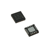
16-WQFN, 16-miniQFN
Operating Temperature
-40°C ~ 85°C
Current - Output / Channel
25mA
Internal Switch(s)
Yes
Efficiency
80%
Lead Free Status / RoHS Status
Lead free / RoHS Compliant
Voltage - Output
-
Lead Free Status / Rohs Status
Details
Other names
LDS8160-002-T2-2


LDS8160
PIN DESCRIPTION
PIN FUNCTION
V
capacitor is required between the V
near the device. The operating input voltage range is
from 2.3 V to 5.5 V.
EN is the enable input for the device. Guaranteed
levels of logic high and logic low are set at 1.3 V and
0.4V respectively. When EN is initially taken high, the
device becomes enabled and can communicate
through I
(initialization) period.
SDAT is the I
line allowing data to be written into and read from the
registers of the LDS8160
SCLK is the I
© 2009 IXYS Corp.
Characteristics subject to change without notice
5, 7, 16
IN
Pin #
PAD
10
11
12
13
14
15
1
2
3
4
6
8
9
is the supply pin. A small 1
2
LEDC2 LEDC2 anode terminal
LEDC1 LEDC1 anode terminal
LEDB2 LEDB2 anode terminal
LEDB1 LEDB1 anode terminal
LEDA2 LEDA2 anode terminal
LEDA1 LEDA1 anode terminal
C interface after a 500 µsec wakeup
Name
SDAT
SADD
SCLK
GND
TST
PAD
EN
V
NC
2
2
C serial clock input.
IN
C serial data line. This is a bidirectional
I
I
I
Ground Reference
Device enable (active high)
Power Source Input; connect to battery or supply
Test pin
Not connect (no internal connect to the device)
Connect to GND on the PCB
2
2
2
C Serial clock input
C Serial data input/output
C Serial interface Addresses Programming
μ
F ceramic bypass
IN
pin and ground
Function
12
SADD is I
pin that allows choice of one of four I
preprogrammed in device.
GND is the ground reference for internal circuitry.
The pin must be connected to the ground plane on
the PCB.
LEDA1 – LEDC2 provide the internal regulated
current sources for each of the LED anodes. These
pins
whenever the device is in shutdown mode.
PAD is the exposed pad underneath the package.
For best thermal performance, the tab should be
soldered to the PCB and connected to the ground
plane
TST is a test pin used by factory only. Leave it
floating (no external connection)
enter
2
C Serial interface Addresses Programming
high-impedance
Top view: TQFN 16-lead 3 X 3 mm
Doc. No. 8160_DS, Rev. N1.0
zero
current
2
C addresses
state
Related parts for LDS8160-002-T2
Image
Part Number
Description
Manufacturer
Datasheet
Request
R

Part Number:
Description:
Dual-output Rgb / 6-channel Wled Driver With Led-sensetm Temperature & Color Compensation
Manufacturer:
IXYS Corporation
Datasheet:

Part Number:
Description:
HiPerFET Power MOSFETs
Manufacturer:
IXYS Corporation
Datasheet:
Part Number:
Description:
J-K-Type Flip-Flop
Manufacturer:
IXYS Corporation
Datasheet:
Part Number:
Description:
HiPerRF Power MOSFETs
Manufacturer:
IXYS Corporation
Datasheet:
Part Number:
Description:
Rectifier Module for Three Phase Power Factor Correction
Manufacturer:
IXYS Corporation
Datasheet:
Part Number:
Description:
Thyristor Modules Thyristor/Diode Modules
Manufacturer:
IXYS Corporation
Datasheet:
Part Number:
Description:
Thyristor Modules Thyristor/Diode Modules
Manufacturer:
IXYS Corporation
Datasheet:
Part Number:
Description:
Thyristor Modules Thyristor/Diode Modules
Manufacturer:
IXYS Corporation
Datasheet:
Part Number:
Description:
Thyristor Modules Thyristor/Diode Modules
Manufacturer:
IXYS Corporation
Datasheet:
Part Number:
Description:
Thyristor Modules /Diode Modules
Manufacturer:
IXYS Corporation
Datasheet:
Part Number:
Description:
Thyristor Modules /Diode Modules
Manufacturer:
IXYS Corporation
Datasheet: